Page
Page
Page
Preface
Page
Table of Contents
Parameters
Troubleshooting
Operation and Start Up
Appendix a Specifications Appendix B Accessories
Fault Code Information and Maintenance
Recommended Position the Rubber Magnet of the Digital Keypad
Appendix C How to Select the Right AC Motor Drive
Introduction
Nameplate Information
Receiving and Inspection
Model Explanation
VFD110VL23A
15HP/5.5-11kWFrame C 20-30HP/15-22kWFrame D
Series Number Explanation
Drive Frames and Appearances
VFD750VL43A
Please refer to .3 for exact dimensions
40-100HP/30-75kWFrame E
Communication Port Internal structure Removable fan
Drive Features
Operation
Preparation for Installation and Wiring Ambient Conditions
Storage
Transportation
15HP/5.5-11kWframe C & 20-30HP/15-22kWframe D
Remove Front Cover
Step
Lifting
40-100HP/30-75kW frame E
Fixed plate Fixed pl ate
Flange Mounting
Fixed plate
15HP/5.5-11kW frame C
Cutout Dimensions
20-30HP/15-22kW frame D
Frame C
Dimensions
Unit mm inch
Frame
Frame D VFD150VL23A/43A, VFD185VL23A/43A, VFD220VL23A/43A
Frame D
255.0 226.0 403.8 384.0 360.0 21.9 168.0 10.04 15.90 15.12
Frame E
This page intentionally left blank
Wiring
Installation and Wiring
Installation and Wiring
Sink NPN mode Source PNP mode
Used with internal power +24Vdc
Used with external power
Run
DC voltage Low voltage level Battery voltage
Valve
EPS detection MI-COM=43 Electromagnetic Valve Drive ready
Grouning terminals
Loops
External Wiring
Brak e res istor
Main Circuit Main Circuit Connection
Pti onal Non-fuse break er
Motor
Output terminals for main circuit U, V, W
Mains power terminals R/L1, S/L2, T/L3
Models
Models Wire Torque Wire Type
Main Circuit Terminals
Position of External Terminals
Torque Wire Type
Control Terminals
REV
OFF
MI1
MI2
Analog input terminals ACI, AUI1, AUI2, ACM
Digital outputs MO1, MO2, MCM
Frame Torque Wire
AWG 0.3-2.1mm2
Terminal 0V/24V Kgf-com1.4 in-lbf AWG 0.051-1.3mm2
Installation and Wiring
Operation Method
Operation and Start Up
RUN
STOP/RESET
KPVL-CC01
Trial Run
Basic parameter settings Motor tuning
Auto-tuning Operations Flow Chart
Explanations for the Auto-tuning Steps
Operation and Start Up
IM motor
Step
PM motor
Step
EMVL-PGABO/ABL
SIN/COS
EMVL-PGABL
EMVL-PGH01/02
Step
Operation and Start Up
Trial run
Operation and Start Up
Operation and Start Up
Operation and Start Up
Parameters
Group 0 System Parameters
Summary of Parameter Settings
Parameter can be set during operation
Focpg Tqcpg Focpm
Vfpg SVC Focpg Tqcpg Focpm
Group 1 Basic Parameters
Vfpg SVC Focpg Tqcpg
Group 2 Digital Input/Output Parameters
By FWD/REV By Enable 02-25
Group 3 Analog Input/Output Parameters
Explanation Settings
03-19
Group 4 Multi-Step Speed Parameters
Group 5 IM Motor Parameters
Group 6 Protection Parameters
~100.0%
Group 7 Special Parameters
Group 8 PM Motor Parameters
Group 9 Communication Parameters
SIN/COS
Group 10 Speed Feedback Control Parameters
Group 11 Advanced Parameters
Group 12 User-defined Parameters
Group 13 View User-defined Parameters
00-01
Description of Parameter Settings
00-00
Content of Multi-Function Display
Factory setting
Factory setting
00-02
SEEEEEEE0 0 HzEE
DOEON/ OFFESt a t
DI EON/ OFFESt a t
FFF
MI8 MI7 MI6 MI5 MI4 MI3 MI2 MI1 REV FWD
Settings Read Only Display #.##
Factory setting Read Only
00-05
User Defined Coefficient K
Password Set Unit
Password Input Unit
Settings To 9998 and 10000 to Display
00-07
00-09Control Method
Decoding Flow Chart
Pass word Setting
00-11
00-10
00-12
230V/460V Series
Source of the Operation Command
Source of the Master Frequency Command
00-14
00-15
01-03
01-01
01-02
01-05
01-04
01-06
01-07
01-10
01-09
Output Frequency Upper Limit Unit
01-11
01-14
01-12
01-16
01-18
01-22
Switch Frequency between 1st/4th Accel/decel Unit
JOG Frequency Unit
01-23
1st/4th Acceleration/Deceleration Switching
01-31
01-29
01-28
Parameters
02-00 Control Circuits of the External Terminal
02-00
02-01
02-03
02-02
02-04
02-05
Settings Functions Descriptions
Eeprom
By Pr.07-28 setting
02-09
MI8 MI7 MI6 MI5 MI4 MI3 MI2 MI1 REV
02-10
02-11
02-12
Settings Control Mode
Settings Functions Descriptions
Active when the warning is detected
Input MI=40
Enable
Multifunction output MO=15
02-23
02-26
02-25
02-27
02-28
02-32
02-31
2 7=S
02-35
02-33
02-34
03-02
03-00
03-01
03-03
Settings 100.0~100.0%
Analog Input Bias 1 AUI1 Unit
03-04
03-06
03-05
03-07
03-08
03-13
03-12
03-14
03-15
03-21
03-18
Analog Output Gain Unit
04-01
04-00
04-02
04-03
05-00
Pr 06 Pr Equivalent circuit for VFD -VL ser ie s
Settings 40 to 120%
Factory setting #.##
05-02
05-03
05-13
05-12
05-15
05-14
05-16
05-17
Core Loss Compensation Unit
Settings To 250%
05-20
06-02
06-00
06-01
06-04
06-03
06-06
06-05
06-07
06-08
Pr.06-09
Pr.06-06
Pr.06-07
06-10
Load
Operation time min
Fac tor %
60Hz
06-16 06-17 06-18 06-19 06-20 06-21
Readings No fault
Parameters
06-30
Setting Method of Fault Output
Bit Fault code
Bit Fault code
06-22
Fault code Bit0 Bit1 Bit2 Bit3 Bit4 Bit5 Bit6 Current Volt
06-23
06-24
Bit1 Bit2 Bit3 Bit4 Bit5 Bit6 Fault code Volt
Bit0 Bit1 Bit2 Bit3 Bit4 Bit5
Fault code Current Volt. OL
06-27
06-26
06-28
06-29
07-01
07-00
07-02
07-03
07-0
07-05
07-06
07-07
07-13
07-11
07-12
07-15
07-14
07-17
07-18
07-20
07-19
07-21
07-22
07-24
07-23
07-25
07-26
300% x 07-29=t
100%
00-01
07-28
Settings No function
08-00Motor Auto Tuning
08-02
Rated Power of Motor Unit
08-04
08-03
08-05
08-06
Parameters
09-00
RS-485 5 NC 6 NC
09-01
09-02
Code Description
Ascii mode
RTU mode
Data
STX
END
Start
5CH
FEH
A0H
F7H
Count by word 02H CRC CHK Low
6FH
AC drive Parameters Command Write only
Content
Address Function
GG means parameter group, nn means parameter number
Content Address Function
Exception
Ascii mode RTU mode
A1H
09-05
SIN/COS+
ABZ
Motor will run Motor won’t run 10-00=5
Settings Disable
Motor will run 10-00=6
10-01
10-04
10-03
10-05
10-06
10-11
10-08
10-09
10-12
10-19
10-18
10-20
10-21
10-24
10-22
10-23
Adjust by requirement
Setting auto gain adjustment Pr.11-00=1
11-00
System Control
11-02
11-01
11-03
11-04
11-06
11-05
11-07
11-08
11-12
11-10
11-11
11-15
11-13
11-14
SEEEEEE6 0 1 2 0 0 Prog
FREQ. Esetpoi NTn t
Umap ADD0 Eeeetee SEEEEE0 8 0 3 0 8 0 3 0
PMSMOTORUB- Emf ET SEEEEEE6 0 1 3 0 0 Prog
SEEEEEE6 0 1 2- 0 0 Prog
FREQ. Esetpoi NTn t SEEEEEE6 0 Hz EEE
EEE- EEn d . E- EEE Eeeeeeeeeeeeeeee
DI SPL AYEUSER- SET SEEEEEE6 0 1 3 0
Systemsparameter press SEEEEEE6 0 0 0 EE twice
FREQ. Esetpoi NTn t SEEEEEE6 0 Hz EEE Prog
Ma x Eo f s Fc md i n t ET SEEEEEE6 0 1 3 0
2127
13-00
Settings Refer to group 12 for details
View User-defined Parameters
13-31
Over Current OC
Troubleshooting
Over Voltage OV
Ground Fault
Ground fault
Low Voltage Lv
Suitable power
Overload
Over Heat OH
Yes
Phase Loss PHL
Display of KPVL-CC01 is Abnormal
Motor cannot Run
Motor Speed cannot be Changed
Motor does not Run as Expected
Motor Stalls during Acceleration
Environmental Condition
Electromagnetic/Induction Noise
Affecting Other Machines
Fault Code Information
Fault Code Information and Maintenance
EEE Fault Co d e 0 E
Common Problems and Solutions
Ea t EAc c e l Eeeee
EEE F a u l t code 0 E3
Motor drive protection, not for protection of the user
EEE Fault Co d e 0 9 E
Display Description Ground fault Corrective Actions
Ea t ES t o p Eeeeee
EEE Fault code 1 E
Eeef a u l t code 2 2 E
EEE Fault code 2 E0
EEE Fault code 3 2 E
EEE Fault code 3 0 E
EEE Fault code 3 E
EEE Fault code 2 E7
EEE Fault Co d e 4 E
FEEEFault code 3 E9
EEE Fault code 4 E
EHWEEr r o r Eeeee
PC EE r r ECo mma n d EE
EEE Fault Co d e 5 E
EEE Fa u l t code 5 E
EEEFa u l t code 5 E6
Eeef a u l t code 6 3 E
Reset
EEE Fault code 5 E
Fault Code Information and Maintenance
Voltage Maintenance Check Items Methods and Criterion
Maintenance and Inspections
Keypad Maintenance Check Items Methods and Criterion
One
Change of copper plate
Main circuit Maintenance Check Items Methods and Criterion
Visual, aural inspection and smell Or peculiar smell
Year
Change fan Overheat
Daily
Daily
This page intentionally left blank
Appendix a Specifications
Per torque 100% Accel up 140% Cruise 80% Decel up Post
General Specifications
This page intentionally left blank
Appendix B Accessories
Decrease accordingly. Recommended cycle time is one minute
All Brake Resistors & Brake Units Used in AC Motor Drives
Appendix B Accessories
Dimensions are in millimeter
Dimensions and Weights for Brake Resistors
Order P/N BR500W030, BR500W100, BR1K0W020, BR1K0W075
Specifications for Brake Unit
189.5 200.0
Dimensions for Brake Unit
121.0 80.0 130.0
VFDB4132
Fuse Specification Chart
Non-fuse Circuit Breaker Chart
Phase Model
Model Recommended Input Current a
142 145 250
110 120 225
130 110 250
160 150 300
AC Output Reactor Recommended Value
AC Reactor AC Input Reactor Recommended Value
Impedance
37.5 52.5 18.5 67.5 82.5 120 100 150 130 195
37.5 52.5 18.5 67.5 120 100 150 130 195 160 240
Applications for AC Reactor
M1 reactor
Correct wiring
AC motor drive
AC motor drive Motor
Silicon rectifier Powerreactor AC motor drive Reactor Motor
Diagram a
Zero Phase Reactor RF220X00A
Diagram B
Nominal Method
460Vac 18.5 Built-in 50/60Hz Phase 110 125 200 100 240
230Vac Built-in 50/60Hz 18.5 110 Phase 125 460V DC Choke
DC Choke Recommended Values
230V DC Choke
Description of the Digital Keypad KPVL-CC01
Digital Keypad KPVL-CC01
=Sto p
=Ru n
Paramecopyeeeeee SEEESAVEE1 Ev 1
Paramecopyeeeeee SEEEREADE1 Eeeeee
Syst Emeparameter S0 EEEEEEEE0 0 EE
EEE- EEr r . E- EEE
To set parameters
How to Operate the Digital Keypad KPVL-CC01
Enter parameter settings
When Read 1 starts blinking, it starts to save to KPVL-CC01
From drive to KPVL-CC01
Press and hold on for about 5 seconds
Recommended Position the Rubber Magnet of the Digital Keypad
Dimension of the Digital Keypad
Specifications
Terminal Symbols
PG Card for Encoder
V, V, W, W
Line driver
Encoder
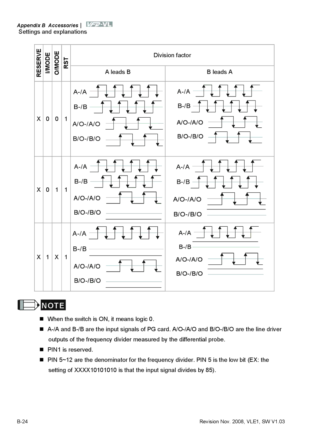
Division Factor
10 11
A/O B/O
A/O
B/O
Power source of encoder
Terminal Symbols Descriptions
Power source common for
TB1
Open collector
A/O, B/O, B/O Z/O
Leads B Leads a A/O B/O
Sinusoidal Encoder Function
EMVL-PGH01 only for Heidenhain ERN1387
SIN COS COS 900mech
+5V Vdc
900el
+ Z
Terminal Symbols Descriptions Specifications
SIN, SIN’
COS, COS’
Leads B Leads a
Division factor
+COS
EMVL-PGS01
Refcos
+SIN
+ +CO S
Encoder
+ +S
Data+
OA-GND
OA-GND OB-GND
Appendix B Accessories
AC Drives Model Number FootPrint
AMD-EMI Filter Cross Reference
50TDS4W4C VFD185VL43A
„ EN61000-6-4 „ EN61800-3 „ EN55011 1991 Class a Group
Length of motor cable
Saddle on both ends Saddle on one end
230VAC input voltage
Dimensions are in millimeter and inch
Order P/N RF110B43CA
Order P/N 50TDS4W4C Order P/N 100TDS84C
Order P/N 200TDDS84C
Order P/N 150TDS84C Order P/N 180TDS84C
AVO1-AGND AVO2-AGND
Max +24V/5mA MO3~MO10 Internal circuit MCM
AVO1 Agnd MO10 MO9 MO8
MCM MO7 MO6 MO5 MO 4 MO3
Relay contact Connect to J P19 On the c ontrol board
Safety Relay EMVL-SAF01 Functions of the Terminals
Wiring of the Safety Relay
Descriptions
This page intentionally left blank
Speed Time Overload Starting Torque Ratings
Related Specification
When one AC motor drive operates more than one motor
When one AC motor drive operates one motor
Capacity Formulas
„ Acceleration time ≧60 seconds Starting capacity=
⋅ IM ≤ the rated current of AC motor drive a
Selection Note
General Precaution
Parameter Settings Note
Standard motor
How to Choose a Suitable Motor
Torque% 25% 40% 60% 100 Continuous Frequency Hz
Pole-changing Dahlander motor
Special motors
Motor torque
Power Transmission Mechanism
This page intentionally left blank