NS7520 Hardware Reference
Page
Part number/version 90000353D Release date March
Page
Contents
A p t e r 4 B B u s M o d u l e
A p t e r 7 M e m o r y C o n t r o l l e r M o d u l e
A p t e r
A p t e r 1 0 S e r i a l C o n t r o l l e r M o d u l e
D e
Who should read this guide
About this guide
What’s in this guide
Conventions used in this guide
To read about See
Related documentation
Documentation updates
Customer support
For Contact information
Page
About the NS7520
Key features and operating modes of the major NS7520 modules
NS7520 Features
O u t t h e N S 7 5 2
7 5 2 0 F e a t u r e s
NS7520 overview
NS7520 module block diagram
Operating frequency
Pinout and Packaging
NS7520 packaging dimensions
Symbol Min Nom Max
Packaging
NS7520 pinout and dimensions
NS7520 BGA layout
Column Description
Pinout detail tables and signal descriptions
System bus interface
Symbol Pin Description
System bus interface pinout
External bus
ADDR6
ADDR7
ADDR5
ADDR4
Do not USE
Signal descriptions
System bus interface signal description
Mnemonic Signal Description
Chip select controller
Chip select controller pinout
Busy
Mnemonic Signal
Chip select controller signal description
Ethernet interface MAC pinout
Ethernet interface MAC
Ethernet interface MAC signal description
CRS
COL
No connect pins
No connect pins
Serial Other Pin Serial channel Signal Description
General-purpose I/O
PORTA3 Rxda DACK1
RTS PORTC4 RXCB/RIB Reset
PORTA2 Dsra Amux
DSR
Serial signal
Gpio signal
Other signal
Serial channel Other Description
System clock and reset
Clock generation and reset signal description
System clock pinout
System mode and system reset pinout
System mode test support
Plltst
Bisten
ARM debugger signal description
Jtag test ARM debugger
Jtag test pinout
Trst termination
Power supply pinout
Power supply
Signal Pin Description
GND
Working with the CPU
CPU performance
ARM Thumb concept
Working with ARM exceptions
ARM mode
ARM performance
ARM
Exception priorities
Summary of ARM exceptions
Exception vector table
Exception vector table
Vector Description Address
Reset exception
Detail of ARM exceptions
Undefined exception
Abort exception
SWI exception
Firq exception
IRQ exception
Entering and exiting an exception software action
Entering an exception
Exiting an exception
Exception entry/exit summary
Reset Undef
Exception entry/exit by exception type
Abort P
Hardware Interrupts
Firq and IRQ lines
Interrupt controller
Interrupt sources
W . d i g i . c o m
Page
BBus Module
Cycles and BBus arbitration
BBus masters and slaves
BBus masters and slaves
Module Master Slave
Address decoding
BBus address decoding
Address range Module
Page
SYS Module
Signal description
Signal mnemonic Signal name Description
Jtag support
ARM debug
System clock generation NS7520 clock module
External oscillator vs. internal PLL circuit
NS7520 clock module block diagram
Using the external oscillator
External oscillator mode hardware configuration
PLL mode hardware configuration
Using the PLL circuit
PLL mode hardware configuration
PLL Settings register Setting the PLL frequency on bootup
Setting the PLL frequency
PLL Settings register bit definition
Bits Access Mnemonic Reset Description D3109 Reserved
MHz A87 A65 A40 ND+1 PLL Settings reg
Bits Access Mnemonic Reset Description
Output divider
PLL multiplier
MHz A87 A65 A40 ND+1 PLL Settings reg
PLL Control register bit definition
Pllcnt
Sysclk frequency
MHz
ND+1 PLL Settings register
Reset circuit sources
Address bit Name Description
NS7520 bootstrap initialization
GEN Module
GEN module address configuration
Module configuration
GEN module hardware initialization
Address Register
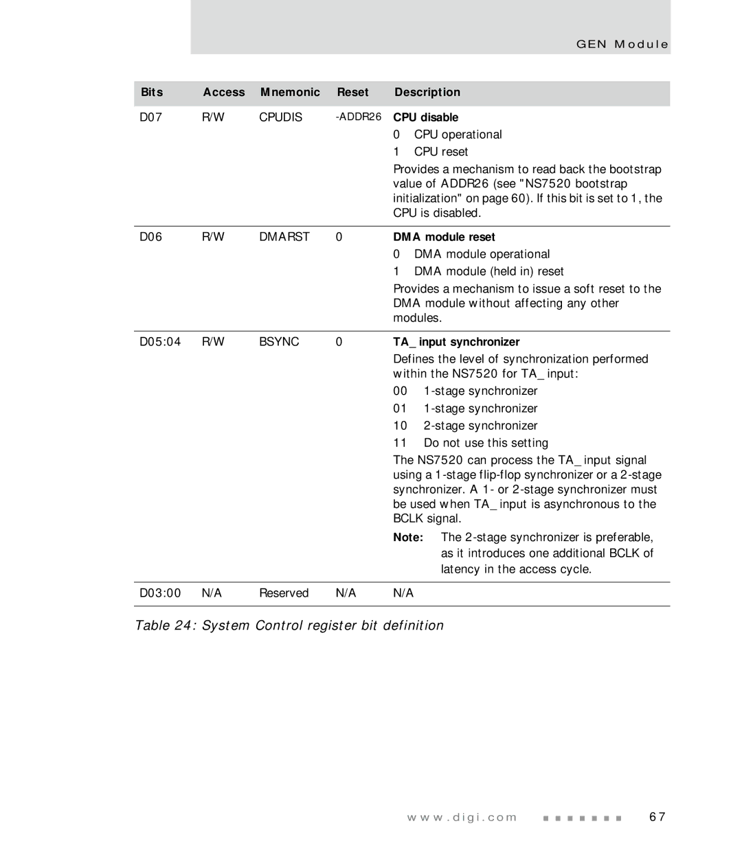
System Control register
GEN module registers
Address FFB0
General information
Software watchdog enable
Bclk output disable
Software watchdog reset/interrupt select
Software watchdog timeout in seconds
Bus monitor enable
Enable access to internal chip registers in CPU
User mode
Description Enable ARM CPU
Bits Access Mnemonic Reset
DMA module test mode
Bus interface TEA/LAST configuration
CPU disable
DMA module reset
TA input synchronizer
System Status register
Last reset caused by external reset
System Status register bit definition
NS7520 revision ID
Last reset caused by PLL update
Last reset caused by watchdog timer
Last reset caused by software reset
Product ID defined by external resistor jumpers
Timer Control registers
Software Service register
Software Service register bit definition
Address FFB0 000C
Timer enable
Timer Control registers bit definition
Timer interrupt enable
Timer interrupt mode
Timer prescaler
Timer clock source
Initial timer count
Timer Status registers bit definition
Timer Status registers
Timer interrupt pending
Current timer count
Porta mode configuration
Porta Configuration register
Porta register bit definition
Porta data direction
Porta configuration
Porta Configuration
Adata
Porta data register
Inputs
PORTA1 Gpio Gpio OUT SER1CTS DONE1OUT PORTA0 SER1SPISENABLE
Outputs
IN/SER1DCD
Portc mode
Portc Configuration register
Portc register bit definition
Portc data direction
Portc configuration
Portc configuration
Cdata
Portc data register
PORTC1 Gpio Gpio OUT LEVELIRQ1=CDIR1 PORTC0 LEVELIRQ0=CDIR0
PORTC30
Interrupts
Address FFB0 0030 / 0034
Interrupt controller registers
Interrupt Enable registers bit definition
D01
Page
Memory Controller Module
MEM module pin configuration by memory type
Pin configuration
Mode A2714 A130 CSx
About the MEM module
Mode A2714 A130
Sdram
RAS CAS
Setting the chip select address range
MEM module configuration
Memory controller register map
Address Mnemonic Register
Memory Space
Enable Dram refresh
Memory Module Configuration register
Mmcr bit definition
Refresh count value
Enable A27 output
Enable external address multiplexing
Rcyc
Refresh cycle count
Enable A26 output
A27 and A26 bit settings
Enable A25 output
AMUX2
Chip Select Base Address register bit definition
Chip Select Base Address register
Base
Base address
Dram configuration mode
Peripheral page size
Dram address multiplexer select
Dram internal address multiplexer mode
External TA configuration
Burst memory cycle enable
Force Bclk at end of memory cycle
Write-protect the chip select
Eeprom
Valid bit
Chip Select Option Register a bit definition
Chip Select Option Register a
Mask
Mask Address
When DRSEL=0
When DRSEL=1 and DMODE=2’b00
When DRSEL=1 and DMODE=2’b01 at full speed
Burst access size in beats
When DRSEL=1 and DMODE=10
Bsize
Port size
Write cycle mode
Read cycle mode
OE Ctrl
WE Ctrl
Chip Select Option Register B bit definition
Chip Select Option Register B
Sync
Static memory Sram controller
Sync Write Sync Read
Single cycle read/write
Async Read
Burst cycles
Using the internal multiplexer
NS7520 Dram address multiplexing
000 001 010 011 100 101 110 111
7 5 2 0 D R a M a d d r e s s m u l t i p l e x i n g
Internal Dram multiplexing Mode
NS7520 multiplexed address outputs
Dram
Using the external multiplexer
FP/EDO Dram controller
Dram refresh
FP Dram Write FP Dram Read
Normal FP Dram bus cycles
FP Dram burst cycles
FP/EDO Dram burst cycles
X32 Sdram configuration
NS7520 Sdram interconnect
X32 Sdram interconnect
BA1
X16 Sdram configuration
BA0
BA1 Bclk CLK VCC CKE
X16 Sdram interconnect
NS7520 signal 16M Sdram signal 64M Sdram signal
CAS3 RAS CAS2 CAS1 CAS0
Udqm
NS7520 signal 16M Sdram signal
X8 Sdram configurations
X8 Sdram interconnect
Bclk CLK VCC CKE
Sdram A10/AP support
Sdram command definitions
Command definitions
Mux mode X32 X16
Command
CAS latency Bcyc configuration
Bsize configuration
Memory timing fields Sdram
Burst length
Sdram Mode register settings
Sdram Mode register
Full
Address Field Value
Sdram normal read
Sdram read cycles
Sdram burst read
Sdram normal write
Sdram write cycles
Sdram burst write
Example
Peripheral page burst size
Wait Bcyc
Page
DMA Module
Fly-by operation transfers
DMA module
DMA fly-by transfers
Memory-to-memory operation
DMA buffer descriptor
DMA buffer descriptor Fly-by mode
Buffer descriptor bit definitions
Buffer descriptor bit definitions
Bit Description
Buffer descriptor field definitions
Buffer descriptor field definitions
Field Description
Channel Base address DMA channel peripheral Fly-by mode
DMA channel assignments
DMA channel assignments
DMA channel registers
Address map
Address Description
Address Description
DMA Control register
Buffer Descriptor Pointer register
DMA operation mode
DMA channel enable
DMA Control register bit definition
Channel abort request
Burst transfer enable
Memory-to-memory mode
BTE
Channel request source
REQ
Source address increment
Sinc
Dinc
Destination address increment
Data operand size
Current DMA channel state shown in binary
Current DMA channel buffer descriptor index
DMA Status/Interrupt Enable register bit definition
DMA Status/Interrupt Enable register
Error completion interrupt pending
Normal completion interrupt pending
Normal completion interrupt enable
Premature complete interrupt enable
Error completion interrupt enable
Buffer not ready interrupt enable
Ethernet transmitter considerations
External peripheral DMA support
Ethernet receiver considerations
External DMA configuration
Signal description
Memory-to-memory mode
Signal Description
Hardware needed for external memory-to-memory DMA transfers
DMA controller reset
Page
Ethernet Module
Fifo
Ethernet front-end EFE
Transmit and receive FIFOs
EFE transmit processing
EFE receive processing
DMA
Receive buffer descriptor selection
External CAM filtering
MAC module
MAC module block diagram
Other modules in the diagram include
EFE configuration
EFE register map
Address Register Register description
Supp
Maxf
Test
Mcfg
Address FF80
Ethernet General Control register Egcr bit definitions
Erxetx Erxdmaetxdma Erxlngetxwm Erxshtefulld Erxbad
Erxregetxreg Erfifohetfifoh Erxbretxbc
Ethernet General Control register bit definition
Enable transmit DMA
Enable transmit Fifo
Do not set this bit when operating the Ethernet
Receiver in interrupt service mode
Enable transmit data Fifo half empty interrupt
Enable Transmit Data register ready interrupt
Enable transmit buffer complete interrupt
Enable full-duplex operation
Invert the transmit clock input
MAC software reset
PSOS pNA buffer descriptors
Insert transmit source address
Endec control signal cross-reference
Endec mode and NS7520 pins
External interface mode
Mode field Output based on EFE CSR bit
Ethernet General Status register Egsr bit definitions
Ethernet General Status register bit definition
Rxfdbrxskip Rxregrtxrege Rxfifohtxfifoh Rxbrtxbc
Receive register ready
Receive Fifo data available
Receive Fifo half full
Receive buffer ready
Transmit register empty
Receive buffer skip
Transmit Fifo half empty
Transmit buffer complete
Ethernet Fifo Data register
Endec status signal cross-reference
Address FF80 0008 / FF80 000C secondary address
Writing to the Ethernet Fifo Data register
Reading from the Ethernet Fifo Data register
Ethernet Fifo Data register bit definition
Ethernet Transmit Status register
Ethernet Transmit Status register bit definition
Fifo data FF80
Broadcast packet transmitted
Packet transmitted OK
Multicast packet transmitted
Transmit abort late collision
Transmit abort excessive deferral
Txaed
Txaec
Transmit abort excessive collisions
Transmit aborted underrun
Txaur
Txaj
Transmit abort jumbo
Txdef
Transmit CRC error
Transmit packet deferred
Txcrc
Ethernet Receive Status register
Txcolc
Transmit collision count
Receive buffer size in bytes
Ethernet Receive Status register bit definition
Receive carrier event previously seen
Receive data violation event previously seen
Receive packet has dribble bit error
Receive packet has CRC error
Receive broadcast packet
Receive multicast packet
Receive packet has code violation
Receive packet is too long
Receive packet is too short
MAC Configuration Register
Rover
Receive overflow
MAC Configuration Register 1 bit definition
Receive enable
RX flow control
Pass ALL receive frames
MAC Configuration Register 2 bit definition
Vlan pad enable
Auto detect pad enable
PAD/CRC enable
CRC enable
PAD operation
Pad operation table
Back-to-Back Inter-Packet-Gap register
Back-to-Back Inter-Packet-Gap register bit definition
Back-to-back inter-packet-gap
Address FF80 040C
Non-Back-to-Back Inter-Packet-Gap register
Non-Back-to-Back Inter-Packet-Gap register bit definition
Non back-to-back inter-packet-gap part
Collision Window/Collision Retry register bit definition
Collision Window/Collision Retry register
Collision window
Retransmission maximum
Maximum Frame register
Maximum Frame register bit definition
Maximum frame length
PHY Support register bit assignment
PHY Support register
Bit mode
Enable Jabber protection
Test register
Address FF80 041C
Test backpressure
Test pause
Shortcut pause quanta
MII Management Configuration register bit definition
MII Management Configuration register
Reset MII management
Clock select
Scani
Clks field settings
Scan increment single scan for read data
Clks field Sysclk ratio MHz example
MII Management Command register bit definition
MII Management Command register
Automatically scan for read data
Single scan for read data
MII Management Address register bit definition
MII Management Address register
MII PHY device address
MII PHY register address
Address FF80 042C
MII Management Write Data register
MII Management Write Data register bit definition
MII write data
MII Management Read Data register
MII Management Read Data register bit definition
MII read data
MII Management Indicators register bit definition
MII Management Indicators register
Read data not valid
Automatically scan for read data in progress
Smii Status register
Station Address registers
Smii Status register bit definition
Station Address Register 1 bit definition
Station Address Register
Station Address Register 2 bit definition
Station address octet
OCTET3
Station Address Register 3 bit definition
OCTET4
OCTET5
Station Address Filter register
Address FF80 05C0
Station Address Filter register bit definition
Multicast hash table entries and bit definitions
Register hash table
Address FF80 05D0
Address FF80 05D4
Address FF80 05DC
Address FF80 05D8
HT2 bit definition
HT3 bit definition
Calculating hash table entries
W . d i g i . c o m
Page
W . d i g i . c o m
Page
Serial Controller Module
RTS, CTS, DTR, DSR, DCD, RI
Supported features
Bit-rate generator
Serial port block diagram
Serial protocols
Uart mode
SPI mode
Transmit Fifo interface
Fifo management
Operating in Endian modes
Terminology What’s being written Value
Receive Fifo interface
Processor interrupts vs. DMA
Using DMA
Using processor interrupts
SPI master mode
Signals
Configuration
SPI master transmitter
SPI master receiver
SPI slave mode
Signals
SPI slave receiver
SPI slave transmitter
SPI slave mode 0 and 1 two-byte transfer
General-purpose I/O configurations
Configuration
Operating Mode Serial Port Maximum Rate
Serial port performance
N f i g u r a t i o n
Serial Channel 1, 2 Control Register a
Serial Channel registers
Address FFD0 0000
Serial Channel Control Register a
Stick parity
Parity enable
Even parity select
Number of stop bits
Remote loopback
Enable the transmitter with active CTS
Local loopback
General-purpose output 1/General-purpose
Data terminal ready active
Enable receive DMA requests
Request-to-send active
Receiver interrupt condition
Enable transmit DMA requests
Receiver interrupt enable bits
Receiver interrupts
Transmitter interrupt condition
Transmitter interrupts
Transmitter interrupt enable bits
Serial Channel 1, 2 Control Register B
Address FFD0 0004
Serial Channel Control Register B bit definition
SCC mode
Enable receive character GAP timer
Rcgt
Bitordr
Enable active RTS only while transmitting
Transmit encoding
Receive data encoding
Differential Manchester 111. a 1 is
Address FFD0 0008
Serial Channel 1, 2 Status Register a
Character Match1
Serial Channel Status Register a bit definition
Character Match2
Character Match3
Character GAP timer
Buffer GAP timer
Bgap
Cgap
DCD
Current ring indicator state
Current data carrier detect state
Current data set ready state
Receive framing error interrupt pending
Receive parity error interrupt pending
Receive break interrupt pending
Receive overrun interrupt pending
Rrdy
Receive register ready interrupt pending
Receive Fifo half-full interrupt pending
Receive buffer closed interrupt pending
Receive Fifo full
Change in RI interrupt pending
Change in DCD interrupt pending
Change in DSR interrupt pending
Change in CTS interrupt pending
Transmit register empty interrupt pending
Transmit Fifo half-empty interrupt pending
Transmit buffer closed interrupt pending
Serial Channel 1, 2 Bit-Rate registers
Address FFD0 000C / 4C
Tempty
Timing mode
Bit-rate generator enable
Serial Channel Bit-Rate register bit definition
Receive clock source
Transmit clock source
Drive receive clock external
Drive transmit clock external
Clkmux
BRG input clock
Transmit clock invert
Receive clock invert
If Dpll is not used but you are using
If Dpll is not used and you are not using
When Dpll is used in the application,
Tdcr
Receive divide clock rate
Rdcr
Transmit internal clock source
Tics
Rics
Receiver internal clock source
With the 18.432MHz crystal using Xtale as the clock source
Max baudrates with different clock sources
Nreg
16X @ 55.296MHz
With the 18.432MHz crystal using Sysclk as the clock source
Serial Channel 1, 2 Fifo registers
X1 mode X8 mode X16 mode
Address FFD0 0010
Bit rate examples
Address FFD0 0014
Serial Channel 1, 2 Receive Buffer Gap Timer
Data
Data
Register diagram and bit assignment
Serial Channel 1, 2 Receive Character Gap Timer
Serial Channel Receive Buffer Gap Timer bit definition
Address FFD0 0018
CT value
Serial Channel Receive Character Gap Timer bit definition
Serial Channel 1, 2 Receive Match Mask register
Serial Channel 1,2 Receive Match register
Address FFD0 001C / 5C
Address FFD0 0020
RMMB1
Serial Channel Receive Match Mask register bit definition
RMMB2
RMMB3
Page
Electrical Characteristics
Recommended operating conditions
DC characteristics
Recommended operating thermal conditions
Sym Parameter Conditions Min Typ Max Unit
Pad pullup and pulldown characteristics
Input/Output characteristics
DC characteristics inputs
DC characteristics outputs
Internal pullup characteristics
AC electrical specifications
AC characteristics
Absolute maximum ratings
Maximum voltage ratings
System loading details
Estimated Signal Load pF Device loads
PORTA3, PORTA1, PORTC3, PORTC1
MDC, MDIO, TXEN, TXER, TXD30
Signal Derating ns/pF
Oscillator Characteristics
Output buffer derating by load capacitance
MDC, TXD30, TXER, TXEN, TDO
NS7520
TimingSpecifications
Timing Diagrams
Resettiming
Reset timing parameters
Num Description Min Typ Max Units
Sram timing
Sram timing parameters
Num Description Min Max Unit
CS* controlled read wait =
Sram read
Sram burst read
CS* controlled read wait = 0, Bcyc =
CS controlled write internal and external, wait =
Sram write
Sram burst write
OE* controlled read wait =
Sram OE read
Sram OE burst read
WE* controlled write wait =
Sram WE write
Sram WE burst write
Sdram timing parameters
Sdram timing
Sdram read, CAS latency =
Sdram read
Active Read Inhibit Prechg Bterm
Sdram burst read
Sdram burst read
Sdram write
Sdram write
Sdram burst write
Sdram burst write
Sdram refresh
Sdram load mode
FP Dram timing parameters
FP Dram timing
Fast Page read
FP Dram read
Fast Page burst read
FP Dram burst read
Fast Page write
FP Dram write
Fast Page burst write
FP Dram burst write
Fast page refresh Rcyc =
Fprefreshcycles
CAS3 CAS2 CAS1 CAS0 RF1 RF2 RF3 RF4 RF5 RF8
Ethernet timing parameters
Ethernet timing
Ethernet cam timing
Ethernet PHY timing
Jtag timing
Jtag arm ice timing diagram
Jtag arm ice timing parameters
Num Description Min Max Units
Jtag bscan timing parameters
Jtag bscan timing diagram
External DMA timing parameters
External DMA timing
Fly-by external DMA
Memory-to-memory external DMA
Serial external timing characteristics
Serial internal timing characteristics
Serial internal/external timing
2T SYS
Synchronous serial external clock
Synchronous serial internal clock
Gpio timing diagram
Gpio timing
Gpio timing parameters
Page
Index
CPU
Non-Back-to-BackInter-Packet-Gap register
FP Dram
Portc
NET+ARM
PORTC0
Receiver interrupts 229 transmitter interrupts
Undefined exception 32
Page