C8051F340/1/2/3/4/5/6/7
13.2. Accessing USB FIFO Space
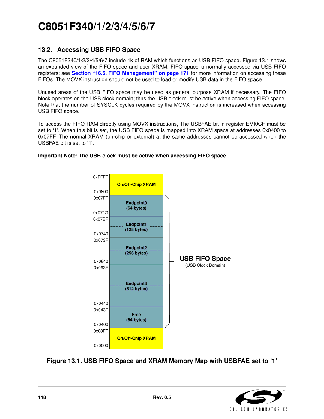
The C8051F340/1/2/3/4/5/6/7 include 1k of RAM which functions as USB FIFO space. Figure 13.1 shows an expanded view of the FIFO space and user XRAM. FIFO space is normally accessed via USB FIFO registers; see Section “16.5. FIFO Management” on page 171 for more information on accessing these FIFOs. The MOVX instruction should not be used to load or modify USB data in the FIFO space.
Unused areas of the USB FIFO space may be used as general purpose XRAM if necessary. The FIFO block operates on the USB clock domain; thus the USB clock must be active when accessing FIFO space. Note that the number of SYSCLK cycles required by the MOVX instruction is increased when accessing USB FIFO space.
To access the FIFO RAM directly using MOVX instructions, The USBFAE bit in register EMI0CF must be set to ‘1’. When this bit is set, the USB FIFO space is mapped into XRAM space at addresses 0x0400 to 0x07FF. The normal XRAM
Important Note: The USB clock must be active when accessing FIFO space.
0xFFFF |
0x0800 |
0x07FF |
Endpoint0 |
(64 bytes) |
0x07C0 |
0x07BF |
Endpoint1 |
(128 bytes) |
0x0740 |
0x073F |
Endpoint2 |
(256 bytes) |
0x0640 |
0x063F |
Endpoint3 |
(512 bytes) |
0x0440 |
0x043F |
Free |
(64 bytes) |
0x0400 |
0x03FF |
0x0000 |
USB FIFO Space
(USB Clock Domain)
Figure 13.1. USB FIFO Space and XRAM Memory Map with USBFAE set to ‘1’
118 | Rev. 0.5 |