C8051F340/1/2/3/4/5/6/7
1.9.10-Bit Analog to Digital Converter
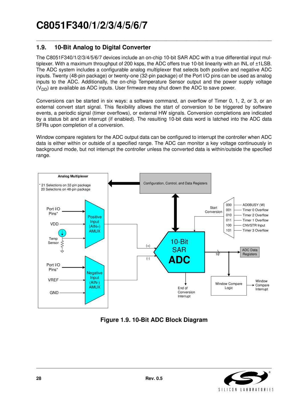
The C8051F340/1/2/3/4/5/6/7 devices include an
Conversions can be started in six ways: a software command, an overflow of Timer 0, 1, 2, or 3, or an external convert start signal. This flexibility allows the start of conversion to be triggered by software events, a periodic signal (timer overflows), or external HW signals. Conversion completions are indicated by a status bit and an interrupt (if enabled). The resulting
Window compare registers for the ADC output data can be configured to interrupt the controller when ADC data is either within or outside of a specified range. The ADC can monitor a key voltage continuously in background mode, but not interrupt the controller unless the converted data is within/outside the specified range.
Analog Multiplexer
* 21 Selections on
Port I/O
Pins*
Positive
Configuration, Control, and Data Registers
Start | 000 | AD0BUSY (W) | |
001 | Timer 0 Overflow | ||
Conversion | |||
|
|
010 | Timer 2 Overflow |
VDD
Input
011 | Timer 1 Overflow |
(AIN+)
AMUX
Temp
Sensor
Port I/O
Pins*
Negative
(+)
SAR
100 |
|
| CNVSTR Input |
| |||
101 |
|
| Timer 3 Overflow |
|
|
| ADC Data |
16 | Registers |
VREF
Input
AMUX
GND
End of
Conversion
Interrupt
Window Compare | Window | |
Compare | ||
Logic | ||
Interrupt | ||
|
Figure 1.9. 10-Bit ADC Block Diagram
28 | Rev. 0.5 |