C8051F340/1/2/3/4/5/6/7
The C/T0 bit (TMOD.2) selects the counter/timer's clock source. When C/T0 is set to logic 1,
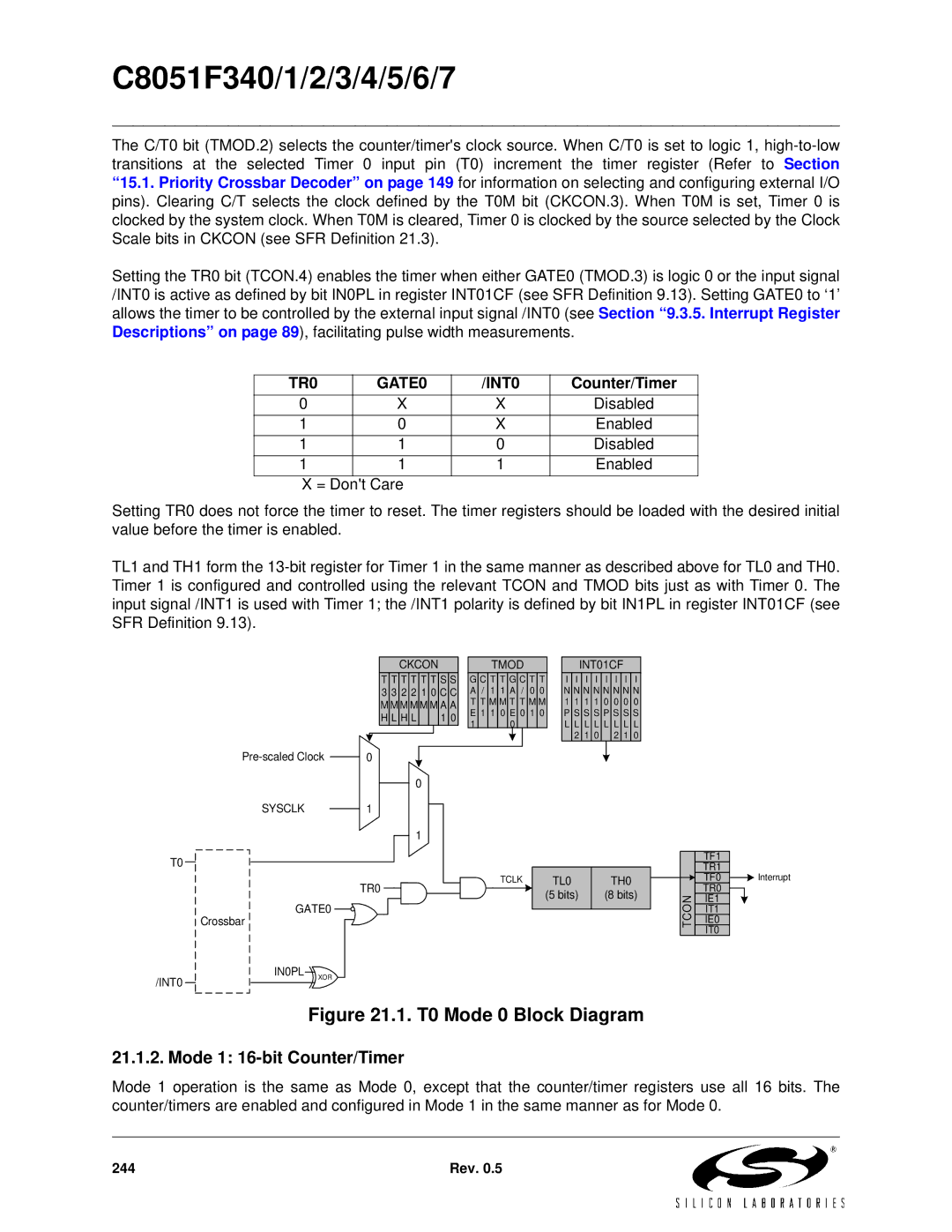
Setting the TR0 bit (TCON.4) enables the timer when either GATE0 (TMOD.3) is logic 0 or the input signal /INT0 is active as defined by bit IN0PL in register INT01CF (see SFR Definition 9.13). Setting GATE0 to ‘1’ allows the timer to be controlled by the external input signal /INT0 (see Section “9.3.5. Interrupt Register Descriptions” on page 89), facilitating pulse width measurements.
TR0 | GATE0 | /INT0 | Counter/Timer |
0 | X | X | Disabled |
1 | 0 | X | Enabled |
1 | 1 | 0 | Disabled |
1 | 1 | 1 | Enabled |
X = Don't Care
Setting TR0 does not force the timer to reset. The timer registers should be loaded with the desired initial value before the timer is enabled.
TL1 and TH1 form the
|
|
| CKCON | |||||
| T | T | T | T | T | T | S | S |
| 3 | 3 | 2 | 2 | 1 | 0 | C | C |
| M | M | M | M | M | M | A | A |
| H | L | H | L |
|
| 1 | 0 |
|
|
|
|
|
|
|
|
|
TMOD
G C T T G C T T A / 1 1 A / 0 0
TT M M T T M M E 1 1 0 E 0 1 0
1 0
INT01CF
I | I | I | I | I | I | I | I |
N | N | N | N | N | N | N | N |
1 | 1 | 1 | 1 | 0 | 0 | 0 | 0 |
P | S | S | S | P | S | S | S |
L | L | L | L | L | L | L | L |
| 2 | 1 | 0 |
| 2 | 1 | 0 |
T0
/INT0
| 0 | |
| ||
|
|
|
0
SYSCLK 1
1
TR0
GATE0
Crossbar
IN0PL![]()
XOR
TCLK
TL0
(5 bits)
TH0
(8 bits)
TCON
TF1 |
|
TR1 |
|
TF0 | Interrupt |
TR0 |
|
IE1 |
|
IT1 |
|
IE0 |
|
IT0 |
|
Figure 21.1. T0 Mode 0 Block Diagram
21.1.2. Mode 1: 16-bit Counter/Timer
Mode 1 operation is the same as Mode 0, except that the counter/timer registers use all 16 bits. The counter/timers are enabled and configured in Mode 1 in the same manner as for Mode 0.
244 | Rev. 0.5 |