C8051F340/1/2/3/4/5/6/7
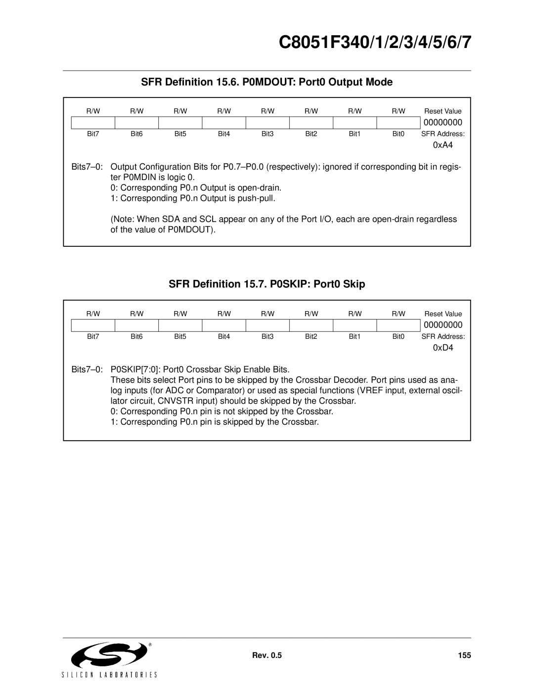
SFR Definition 15.6. P0MDOUT: Port0 Output Mode
R/W | R/W | R/W | R/W | R/W | R/W | R/W | R/W |
| Reset Value |
|
|
|
|
|
|
|
| 00000000 | |
Bit7 | Bit6 | Bit5 | Bit4 | Bit3 | Bit2 | Bit1 | Bit0 |
| SFR Address: |
|
|
|
|
|
|
|
|
| 0xA4 |
0: Corresponding P0.n Output is
1: Corresponding P0.n Output is
(Note: When SDA and SCL appear on any of the Port I/O, each are
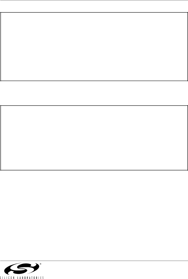
SFR Definition 15.7. P0SKIP: Port0 Skip
R/W | R/W | R/W | R/W | R/W | R/W | R/W | R/W | Reset Value |
|
|
|
|
|
|
|
| 00000000 |
Bit7 | Bit6 | Bit5 | Bit4 | Bit3 | Bit2 | Bit1 | Bit0 | SFR Address: |
0xD4
These bits select Port pins to be skipped by the Crossbar Decoder. Port pins used as ana- log inputs (for ADC or Comparator) or used as special functions (VREF input, external oscil- lator circuit, CNVSTR input) should be skipped by the Crossbar.
0: Corresponding P0.n pin is not skipped by the Crossbar.
1: Corresponding P0.n pin is skipped by the Crossbar.
Rev. 0.5 | 155 |