C8051F340/1/2/3/4/5/6/7
| CMXnN2 | |
CPTnMX | CMXnN1 | |
CMXnN0 | ||
CMXnP2 | ||
| ||
| CMXnP1 | |
| CMXnP0 |
| CPnEN |
|
| CPnOUT |
|
CPTnCN | CPnRIF | VDD |
CPnFIF |
| |
|
| |
| CPnHYP1 |
|
| CPnHYP0 |
|
| CPnHYN1 |
|
| CPnHYN0 |
|
CPn
Interrupt
CPnCPn
CPn +
![]() +
+
![]() -
-
GND
CPn -
D SET Q |
| D SET | Q |
| |||
CLR Q |
| CLR | Q |
(SYNCHRONIZER)
Interrupt CPnRIE
Logic CPnFIE
CPn
Crossbar
CPnA
Port I/O connection options vary with package
CPTnMD | CPnRIE |
CPnFIE | |
| |
| CPnMD1 |
| CPnMD0 |
Reset Decision Tree (Comprator 0 Only)
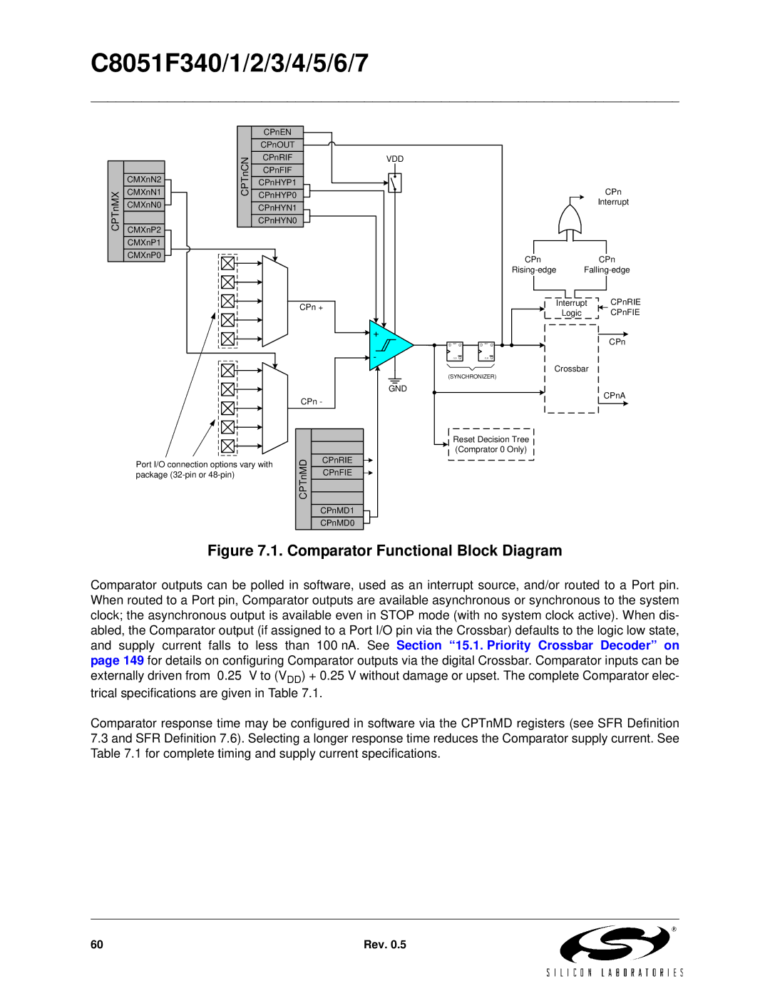
Figure 7.1. Comparator Functional Block Diagram
Comparator outputs can be polled in software, used as an interrupt source, and/or routed to a Port pin. When routed to a Port pin, Comparator outputs are available asynchronous or synchronous to the system clock; the asynchronous output is available even in STOP mode (with no system clock active). When dis- abled, the Comparator output (if assigned to a Port I/O pin via the Crossbar) defaults to the logic low state, and supply current falls to less than 100 nA. See Section “15.1. Priority Crossbar Decoder” on page 149 for details on configuring Comparator outputs via the digital Crossbar. Comparator inputs can be externally driven from
Comparator response time may be configured in software via the CPTnMD registers (see SFR Definition
7.3and SFR Definition 7.6). Selecting a longer response time reduces the Comparator supply current. See Table 7.1 for complete timing and supply current specifications.
60 | Rev. 0.5 |