C8051F340/1/2/3/4/5/6/7
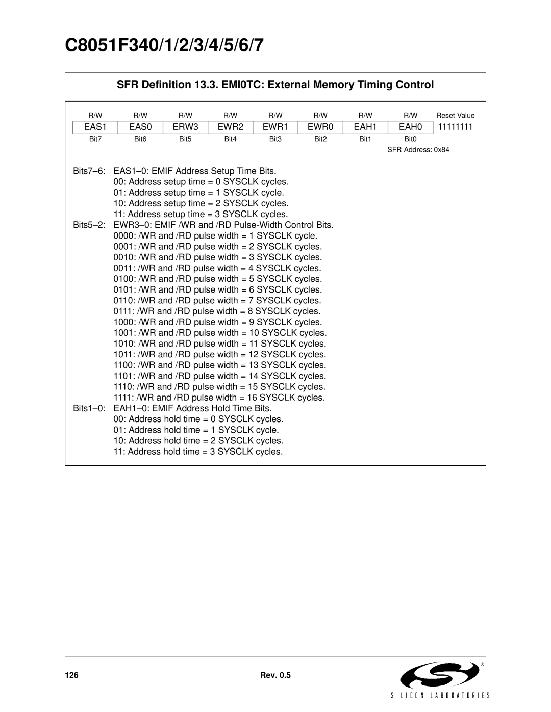
SFR Definition 13.3. EMI0TC: External Memory Timing Control
R/W | R/W | R/W | R/W | R/W | R/W | R/W | R/W | Reset Value |
EAS1
EAS0
ERW3
EWR2
EWR1
EWR0
EAH1
EAH0
11111111
Bit7 | Bit6 | Bit5 | Bit4 | Bit3 | Bit2 | Bit1 | Bit0 |
SFR Address: 0x84
00:Address setup time = 0 SYSCLK cycles.
01:Address setup time = 1 SYSCLK cycle.
10:Address setup time = 2 SYSCLK cycles.
11:Address setup time = 3 SYSCLK cycles.
0001: /WR and /RD pulse width = 2 SYSCLK cycles.
0010: /WR and /RD pulse width = 3 SYSCLK cycles.
0011: /WR and /RD pulse width = 4 SYSCLK cycles.
0100: /WR and /RD pulse width = 5 SYSCLK cycles.
0101: /WR and /RD pulse width = 6 SYSCLK cycles.
0110: /WR and /RD pulse width = 7 SYSCLK cycles.
0111: /WR and /RD pulse width = 8 SYSCLK cycles.
1000: /WR and /RD pulse width = 9 SYSCLK cycles.
1001: /WR and /RD pulse width = 10 SYSCLK cycles.
1010: /WR and /RD pulse width = 11 SYSCLK cycles.
1011: /WR and /RD pulse width = 12 SYSCLK cycles.
1100: /WR and /RD pulse width = 13 SYSCLK cycles.
1101: /WR and /RD pulse width = 14 SYSCLK cycles.
1110: /WR and /RD pulse width = 15 SYSCLK cycles.
1111: /WR and /RD pulse width = 16 SYSCLK cycles.
00:Address hold time = 0 SYSCLK cycles.
01:Address hold time = 1 SYSCLK cycle.
10:Address hold time = 2 SYSCLK cycles.
11:Address hold time = 3 SYSCLK cycles.
126 | Rev. 0.5 |