C8051F340/1/2/3/4/5/6/7
8.Voltage Regulator (REG0)
C8051F340/1/2/3/4/5/6/7 devices include a voltage regulator (REG0). When enabled, the REG0 output appears on the VDD pin and can be used to power external devices. REG0 can be enabled/disabled by software using bit REGEN in register REG0CN. See Table 8.1 for REG0 electrical characteristics.
Note that the VBUS signal must be connected to the VBUS pin when using the device in a USB network. The VBUS signal should only be connected to the REGIN pin when operating the device as a
8.1.Regulator Mode Selection
REG0 offers a low power mode intended for use when the device is in suspend mode. In this low power mode, the REG0 output remains as specified; however the REG0 dynamic performance (response time) is degraded. See Table 8.1 for normal and low power mode supply current specifications. The REG0 mode selection is controlled via the REGMOD bit in register REG0CN.
8.2.VBUS Detection
When the USB Function Controller is used (see section Section “16. Universal Serial Bus Controller (USB0)” on page 163), the VBUS signal should be connected to the VBUS pin. The VBSTAT bit (register REG0CN) indicates the current logic level of the VBUS signal. If enabled, a VBUS interrupt will be gener- ated when the VBUS signal matches the polarity selected by the VBPOL bit in register REG0CN. The VBUS interrupt is
Important Note: When USB is selected as a reset source, a system reset will be generated when the VBUS signal matches the polarity selected by the VBPOL bit. See Section “11. Reset Sources” on page 101 for details on selecting USB as a reset source
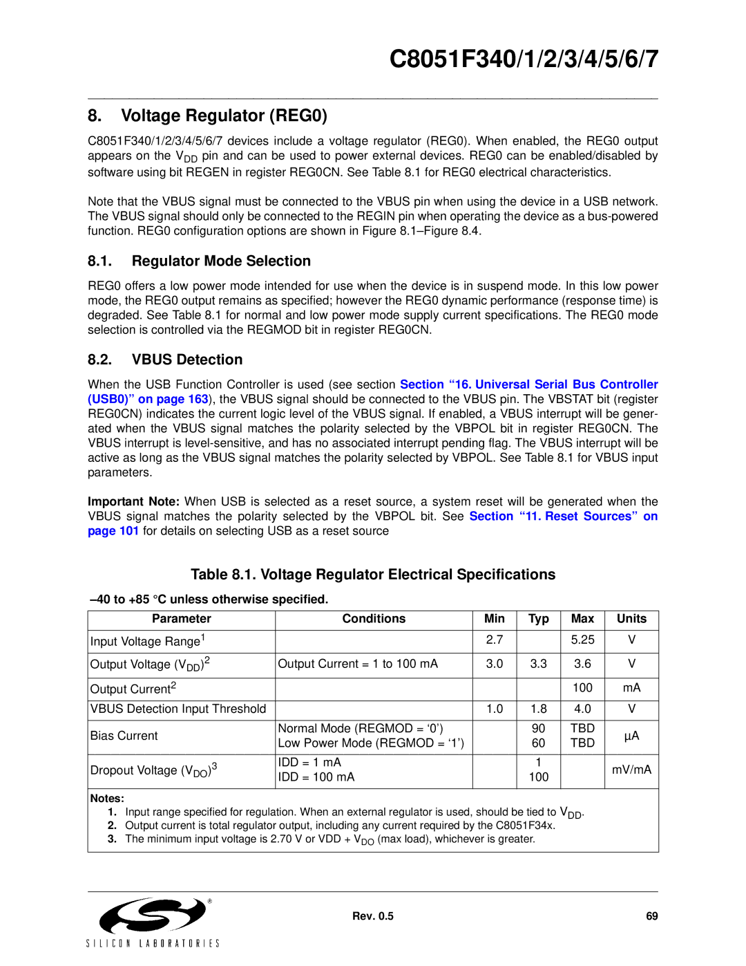
Table 8.1. Voltage Regulator Electrical Specifications
Parameter | Conditions | Min | Typ | Max | Units | |||
|
|
|
|
|
|
| ||
Input Voltage Range1 |
|
| 2.7 |
| 5.25 | V | ||
Output Voltage (V |
| )2 | Output Current = 1 to 100 mA | 3.0 | 3.3 | 3.6 | V | |
DD |
|
|
|
|
|
|
| |
Output Current2 |
|
|
|
|
|
| 100 | mA |
VBUS Detection Input Threshold |
| 1.0 | 1.8 | 4.0 | V | |||
|
|
|
|
|
|
|
|
|
Bias Current |
|
|
| Normal Mode (REGMOD = ‘0’) |
| 90 | TBD | µA |
|
|
| Low Power Mode (REGMOD = ‘1’) |
| 60 | TBD | ||
|
|
|
|
|
| |||
|
|
|
|
|
|
|
|
|
Dropout Voltage (V | DO | )3 | IDD = 1 mA |
| 1 |
| mV/mA | |
IDD = 100 mA |
| 100 |
| |||||
|
|
|
|
| ||||
|
|
|
|
|
|
|
|
|
Notes:
1.Input range specified for regulation. When an external regulator is used, should be tied to VDD.
2.Output current is total regulator output, including any current required by the C8051F34x.
3.The minimum input voltage is 2.70 V or VDD + VDO (max load), whichever is greater.
Rev. 0.5 | 69 |