C8051F340/1/2/3/4/5/6/7
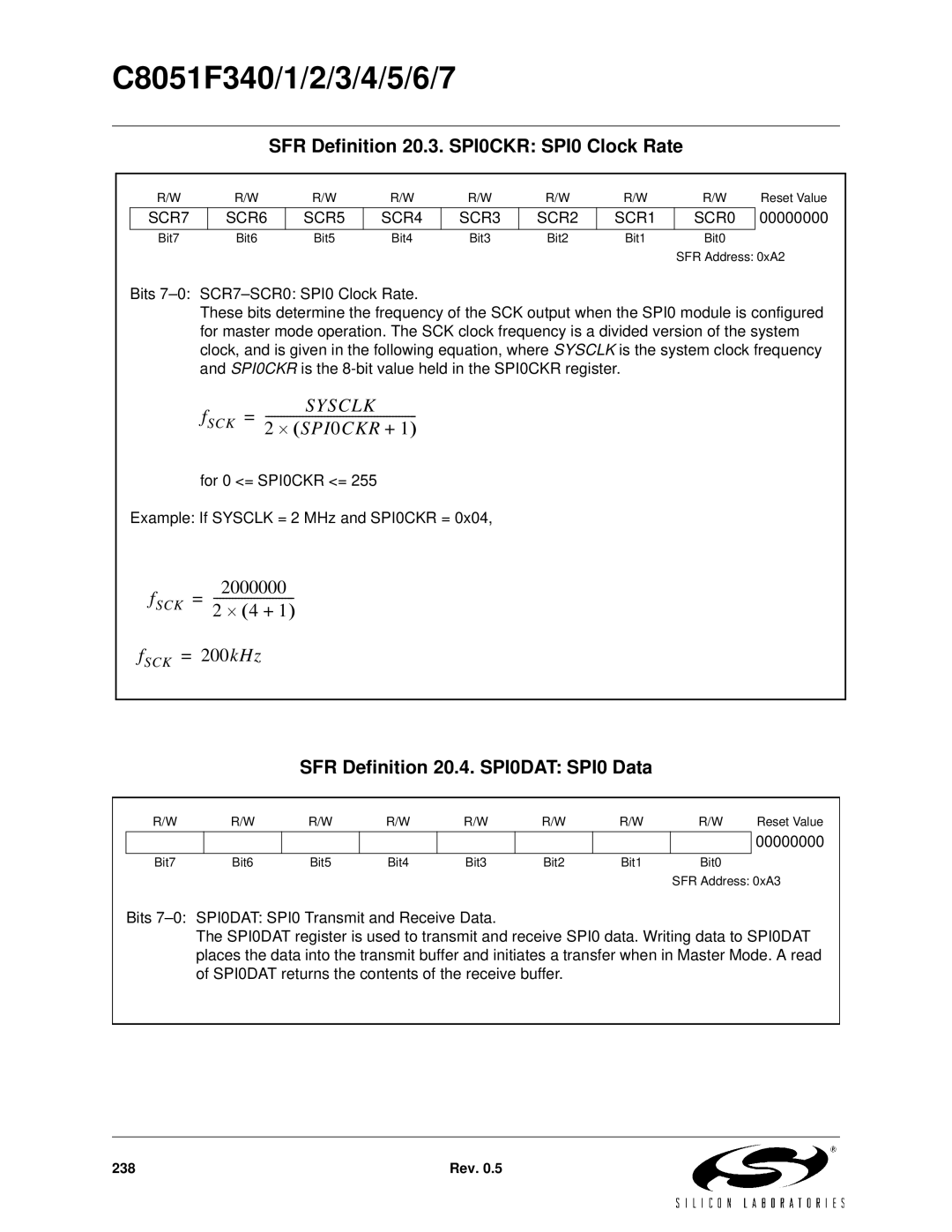
SFR Definition 20.3. SPI0CKR: SPI0 Clock Rate
R/W | R/W | R/W | R/W | R/W | R/W | R/W | R/W | Reset Value |
SCR7
SCR6
SCR5
SCR4
SCR3
SCR2
SCR1
SCR0 00000000
Bit7 | Bit6 | Bit5 | Bit4 | Bit3 | Bit2 | Bit1 | Bit0 |
SFR Address: 0xA2
Bits
These bits determine the frequency of the SCK output when the SPI0 module is configured for master mode operation. The SCK clock frequency is a divided version of the system clock, and is given in the following equation, where SYSCLK is the system clock frequency and SPI0CKR is the
SYSCLK
f =
SCK 2 ⋅ (SPI0CKR + 1)
for 0 <= SPI0CKR <= 255
Example: If SYSCLK = 2 MHz and SPI0CKR = 0x04,
2000000 f =
SCK 2 ⋅ (4 + 1) fSCK = 200kHz
SFR Definition 20.4. SPI0DAT: SPI0 Data
R/W | R/W | R/W | R/W | R/W | R/W | R/W | R/W | Reset Value |
|
|
|
|
|
|
|
| 00000000 |
Bit7 | Bit6 | Bit5 | Bit4 | Bit3 | Bit2 | Bit1 | Bit0 |
|
SFR Address: 0xA3
Bits
The SPI0DAT register is used to transmit and receive SPI0 data. Writing data to SPI0DAT places the data into the transmit buffer and initiates a transfer when in Master Mode. A read of SPI0DAT returns the contents of the receive buffer.
238 | Rev. 0.5 |