Silicon Laboratories C8051F345, C8051F347 Bit Uart Timing Diagram Multiprocessor Communications

Models: C8051F346 C8051F347 C8051F344 C8051F342 C8051F343 C8051F345 C8051F340 C8051F341

1 282
Download 282 pages 2.89 Kb
Page 214
Image 214

C8051F340/1/2/3/4/5/6/7

18.2.2. 9-Bit UART

9-bit UART mode uses a total of eleven bits per data byte: a start bit, 8 data bits (LSB first), a programma- ble ninth data bit, and a stop bit. The state of the ninth transmit data bit is determined by the value in TB80 (SCON0.3), which is assigned by user software. It can be assigned the value of the parity flag (bit P in reg- ister PSW) for error detection, or used in multiprocessor communications. On receive, the ninth data bit goes into RB80 (SCON0.2) and the stop bit is ignored.

Data transmission begins when an instruction writes a data byte to the SBUF0 register. The TI0 Transmit Interrupt Flag (SCON0.1) is set at the end of the transmission (the beginning of the stop-bit time). Data reception can begin any time after the REN0 Receive Enable bit (SCON0.4) is set to ‘1’. After the stop bit is received, the data byte will be loaded into the SBUF0 receive register if the following conditions are met:

(1)RI0 must be logic 0, and (2) if MCE0 is logic 1, the 9th bit must be logic 1 (when MCE0 is logic 0, the state of the ninth data bit is unimportant). If these conditions are met, the eight bits of data are stored in SBUF0, the ninth bit is stored in RB80, and the RI0 flag is set to ‘1’. If the above conditions are not met, SBUF0 and RB80 will not be loaded and the RI0 flag will not be set to ‘1’. A UART0 interrupt will occur if enabled when either TI0 or RI0 is set to ‘1’.
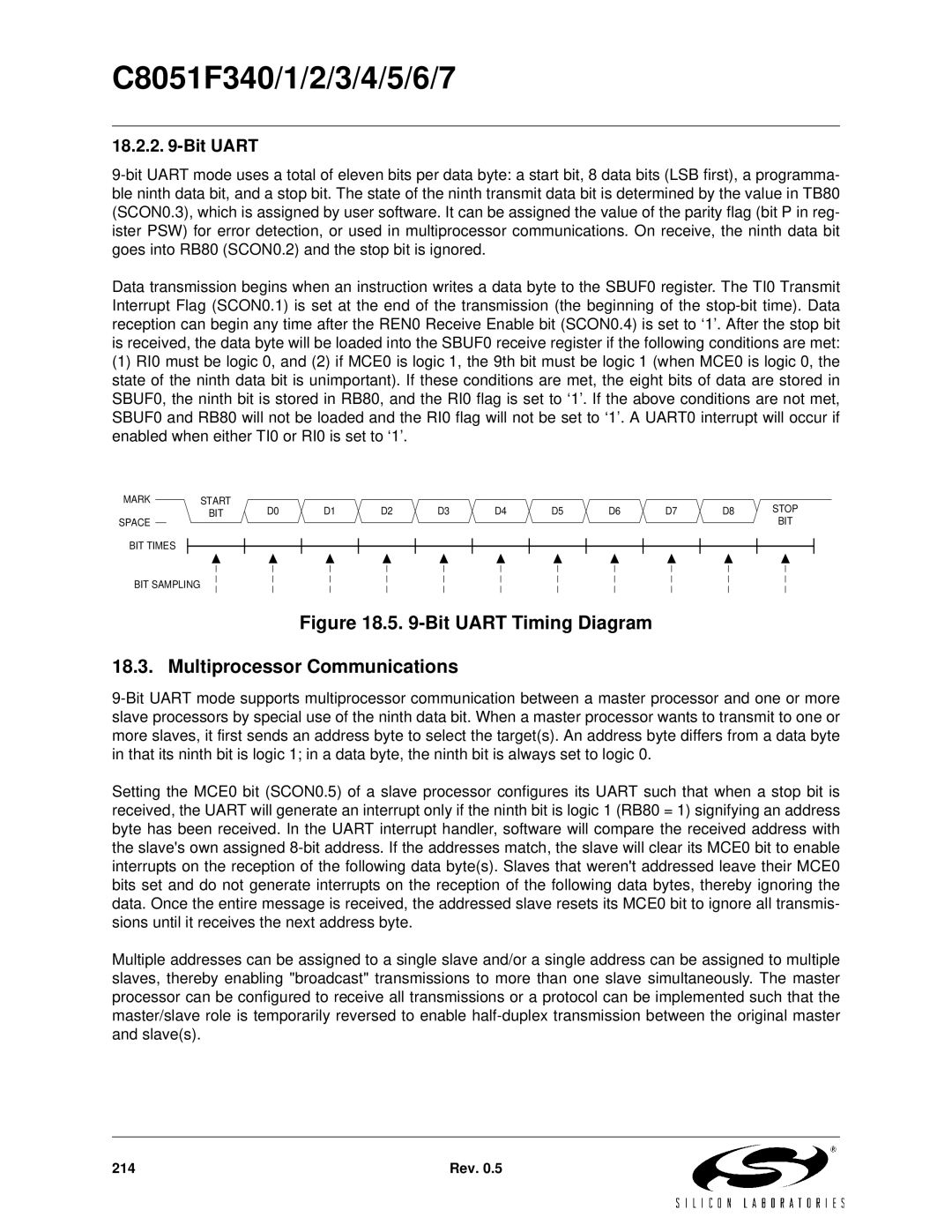
MARK

START

D0

D1

D2

D3

D4

D5

D6

D7

D8

STOP

SPACE

BIT


BIT

BIT TIMES

BIT SAMPLING

Figure 18.5. 9-Bit UART Timing Diagram

18.3. Multiprocessor Communications

9-Bit UART mode supports multiprocessor communication between a master processor and one or more slave processors by special use of the ninth data bit. When a master processor wants to transmit to one or more slaves, it first sends an address byte to select the target(s). An address byte differs from a data byte in that its ninth bit is logic 1; in a data byte, the ninth bit is always set to logic 0.

Setting the MCE0 bit (SCON0.5) of a slave processor configures its UART such that when a stop bit is received, the UART will generate an interrupt only if the ninth bit is logic 1 (RB80 = 1) signifying an address byte has been received. In the UART interrupt handler, software will compare the received address with the slave's own assigned 8-bit address. If the addresses match, the slave will clear its MCE0 bit to enable interrupts on the reception of the following data byte(s). Slaves that weren't addressed leave their MCE0 bits set and do not generate interrupts on the reception of the following data bytes, thereby ignoring the data. Once the entire message is received, the addressed slave resets its MCE0 bit to ignore all transmis- sions until it receives the next address byte.

Multiple addresses can be assigned to a single slave and/or a single address can be assigned to multiple slaves, thereby enabling "broadcast" transmissions to more than one slave simultaneously. The master processor can be configured to receive all transmissions or a protocol can be implemented such that the master/slave role is temporarily reversed to enable half-duplex transmission between the original master and slave(s).

214

Rev. 0.5

Page 214
Image 214
Silicon Laboratories C8051F345, C8051F347, C8051F346, C8051F341 Bit Uart Timing Diagram Multiprocessor Communications