C8051F340/1/2/3/4/5/6/7
15.3. General Purpose Port I/O
Port pins that remain unassigned by the Crossbar and are not used by analog peripherals can be used for general purpose I/O. Ports
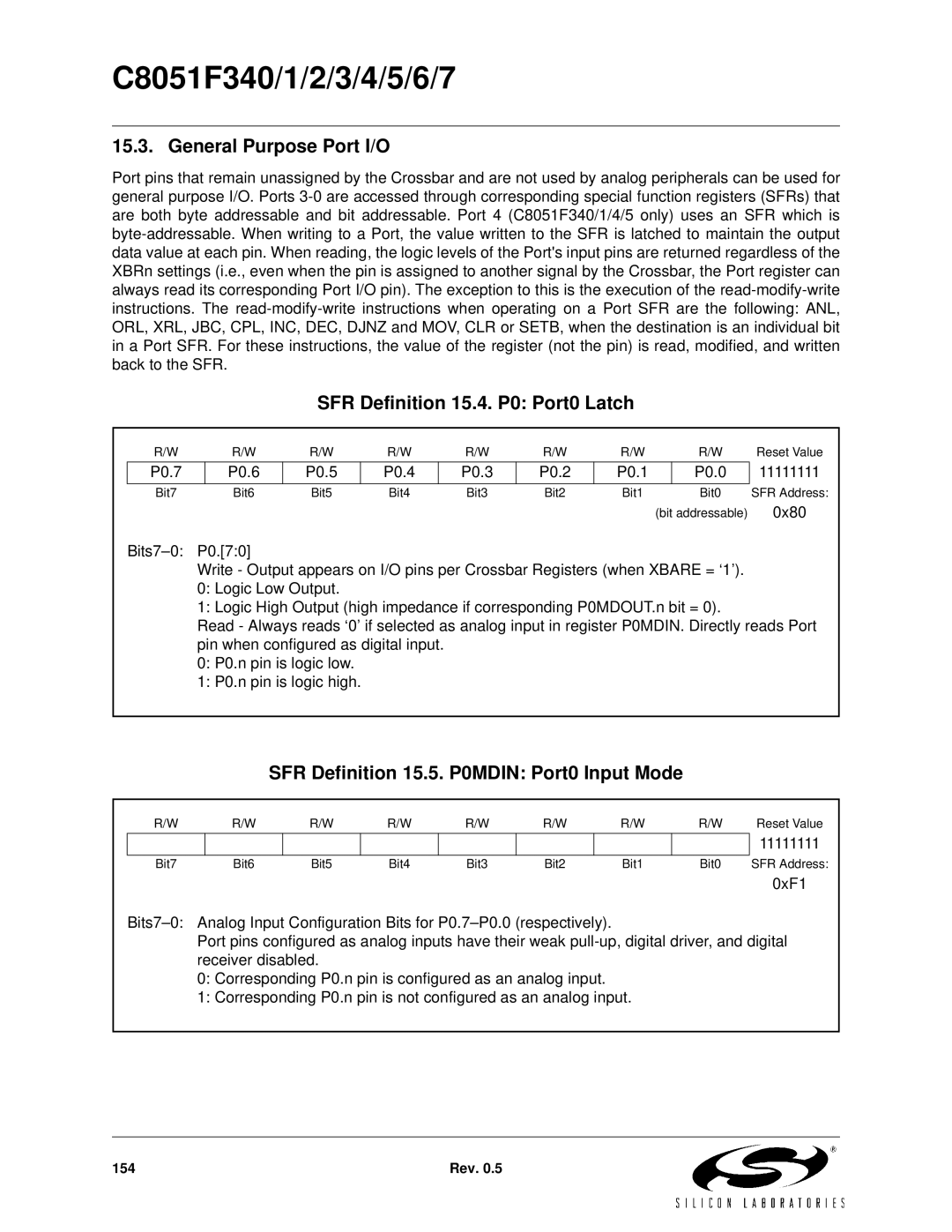
SFR Definition 15.4. P0: Port0 Latch
R/W |
| R/W | R/W | R/W | R/W | R/W | R/W |
| R/W | Reset Value |
P0.7 |
| P0.6 | P0.5 | P0.4 | P0.3 | P0.2 | P0.1 |
| P0.0 | 11111111 |
Bit7 |
| Bit6 | Bit5 | Bit4 | Bit3 | Bit2 | Bit1 |
| Bit0 | SFR Address: |
|
|
|
|
|
|
|
| (bit addressable) | 0x80 | |
P0.[7:0] |
|
|
|
|
|
|
|
| ||
| Write - Output appears on I/O pins per Crossbar Registers (when XBARE = ‘1’). |
| ||||||||
| 0: Logic Low Output. |
|
|
|
|
|
|
| ||
| 1: Logic High Output (high impedance if corresponding P0MDOUT.n bit = 0). |
| ||||||||
Read - Always reads ‘0’ if selected as analog input in register P0MDIN. Directly reads Port pin when configured as digital input.
0: P0.n pin is logic low.
1: P0.n pin is logic high.
SFR Definition 15.5. P0MDIN: Port0 Input Mode
R/W | R/W | R/W | R/W | R/W | R/W | R/W | R/W |
| Reset Value |
|
|
|
|
|
|
|
| 11111111 | |
Bit7 | Bit6 | Bit5 | Bit4 | Bit3 | Bit2 | Bit1 | Bit0 |
| SFR Address: |
0xF1
Port pins configured as analog inputs have their weak
0: Corresponding P0.n pin is configured as an analog input.
1: Corresponding P0.n pin is not configured as an analog input.
154 | Rev. 0.5 |