C8051F340/1/2/3/4/5/6/7
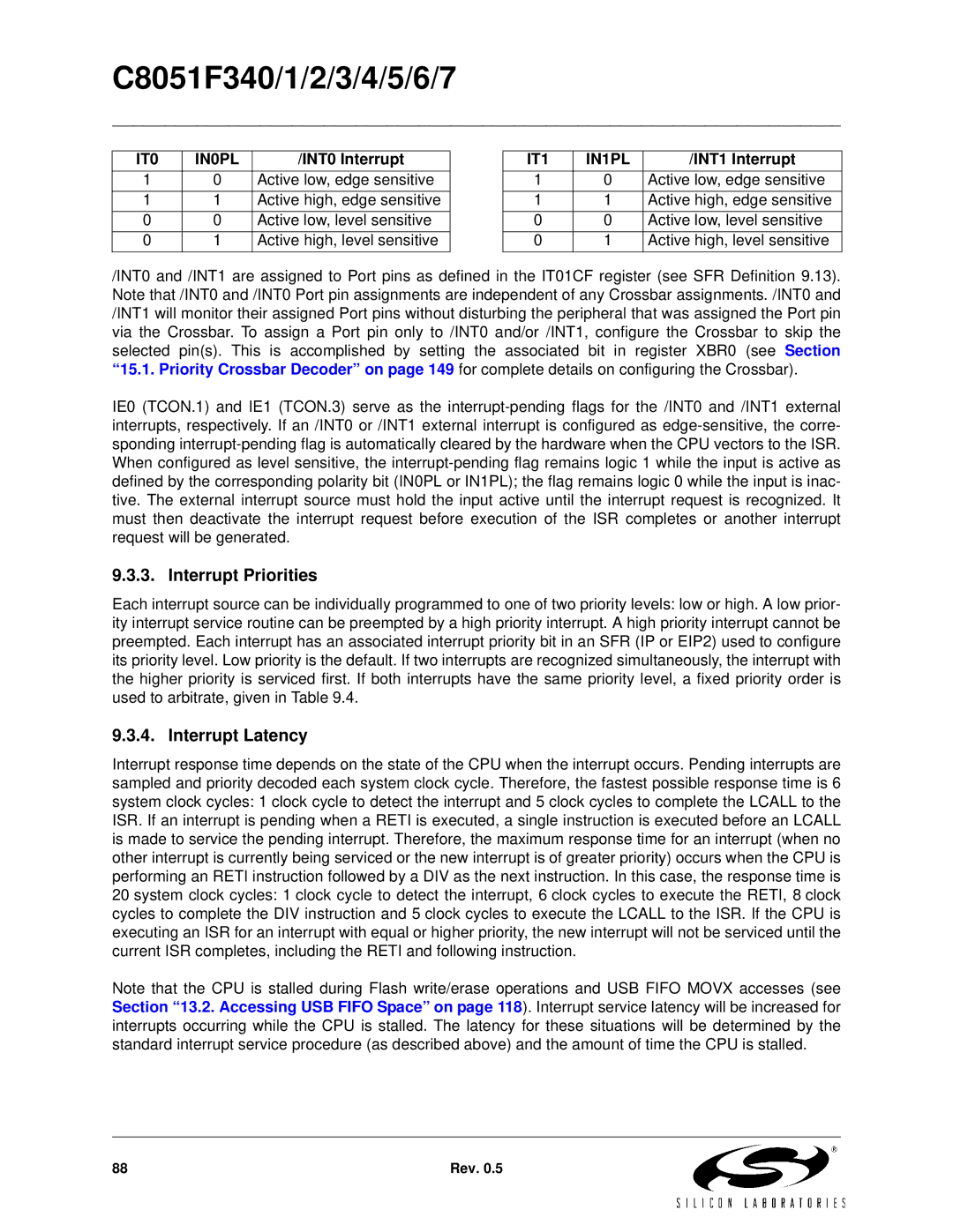
IT0 | IN0PL | /INT0 Interrupt |
1 | 0 | Active low, edge sensitive |
1 | 1 | Active high, edge sensitive |
0 | 0 | Active low, level sensitive |
0 | 1 | Active high, level sensitive |
IT1 | IN1PL | /INT1 Interrupt |
1 | 0 | Active low, edge sensitive |
1 | 1 | Active high, edge sensitive |
0 | 0 | Active low, level sensitive |
0 | 1 | Active high, level sensitive |
/INT0 and /INT1 are assigned to Port pins as defined in the IT01CF register (see SFR Definition 9.13). Note that /INT0 and /INT0 Port pin assignments are independent of any Crossbar assignments. /INT0 and /INT1 will monitor their assigned Port pins without disturbing the peripheral that was assigned the Port pin via the Crossbar. To assign a Port pin only to /INT0 and/or /INT1, configure the Crossbar to skip the selected pin(s). This is accomplished by setting the associated bit in register XBR0 (see Section “15.1. Priority Crossbar Decoder” on page 149 for complete details on configuring the Crossbar).
IE0 (TCON.1) and IE1 (TCON.3) serve as the
9.3.3. Interrupt Priorities
Each interrupt source can be individually programmed to one of two priority levels: low or high. A low prior- ity interrupt service routine can be preempted by a high priority interrupt. A high priority interrupt cannot be preempted. Each interrupt has an associated interrupt priority bit in an SFR (IP or EIP2) used to configure its priority level. Low priority is the default. If two interrupts are recognized simultaneously, the interrupt with the higher priority is serviced first. If both interrupts have the same priority level, a fixed priority order is used to arbitrate, given in Table 9.4.
9.3.4. Interrupt Latency
Interrupt response time depends on the state of the CPU when the interrupt occurs. Pending interrupts are sampled and priority decoded each system clock cycle. Therefore, the fastest possible response time is 6 system clock cycles: 1 clock cycle to detect the interrupt and 5 clock cycles to complete the LCALL to the ISR. If an interrupt is pending when a RETI is executed, a single instruction is executed before an LCALL is made to service the pending interrupt. Therefore, the maximum response time for an interrupt (when no other interrupt is currently being serviced or the new interrupt is of greater priority) occurs when the CPU is performing an RETI instruction followed by a DIV as the next instruction. In this case, the response time is 20 system clock cycles: 1 clock cycle to detect the interrupt, 6 clock cycles to execute the RETI, 8 clock cycles to complete the DIV instruction and 5 clock cycles to execute the LCALL to the ISR. If the CPU is executing an ISR for an interrupt with equal or higher priority, the new interrupt will not be serviced until the current ISR completes, including the RETI and following instruction.
Note that the CPU is stalled during Flash write/erase operations and USB FIFO MOVX accesses (see Section “13.2. Accessing USB FIFO Space” on page 118). Interrupt service latency will be increased for interrupts occurring while the CPU is stalled. The latency for these situations will be determined by the standard interrupt service procedure (as described above) and the amount of time the CPU is stalled.
88 | Rev. 0.5 |