C8051F340/1/2/3/4/5/6/7
19.3. Configuration and Operation
UART1 provides standard asynchronous, full duplex communication. It can operate in a
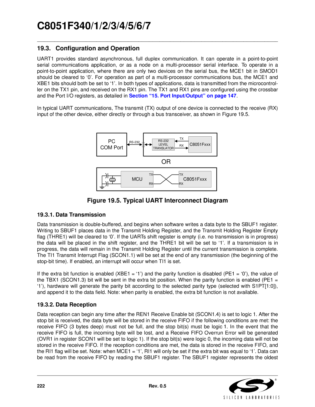
In typical UART communications, The transmit (TX) output of one device is connected to the receive (RX) input of the other device, either directly or through a bus transceiver, as shown in Figure 19.5.
PC
COM Port
TX |
| |
| C8051Fxxx | |
LEVEL | RX | |
TRANSLATOR |
|
|
OR |
|
|
TX | TX |
MCU | C8051Fxxx |
RX | RX |
Figure 19.5. Typical UART Interconnect Diagram
19.3.1. Data Transmission
Data transmission is
If the extra bit function is enabled (XBE1 = ‘1’) and the parity function is disabled (PE1 = ‘0’), the value of the TBX1 (SCON1.3) bit will be sent in the extra bit position. When the parity function is enabled (PE1 = ‘1’), hardware will generate the parity bit according to the selected parity type (selected with S1PT[1:0]), and append it to the data field. Note: when parity is enabled, the extra bit function is not available.
19.3.2. Data Reception
Data reception can begin any time after the REN1 Receive Enable bit (SCON1.4) is set to logic 1. After the stop bit is received, the data byte will be stored in the receive FIFO if the following conditions are met: the receive FIFO (3 bytes deep) must not be full, and the stop bit(s) must be logic 1. In the event that the receive FIFO is full, the incoming byte will be lost, and a Receive FIFO Overrun Error will be generated (OVR1 in register SCON1 will be set to logic 1). If the stop bit(s) were logic 0, the incoming data will not be stored in the receive FIFO. If the reception conditions are met, the data is stored in the receive FIFO, and the RI1 flag will be set. Note: when MCE1 = ‘1’, RI1 will only be set if the extra bit was equal to ‘1’. Data can be read from the receive FIFO by reading the SBUF1 register. The SBUF1 register represents the oldest
222 | Rev. 0.5 |