C8051F340/1/2/3/4/5/6/7
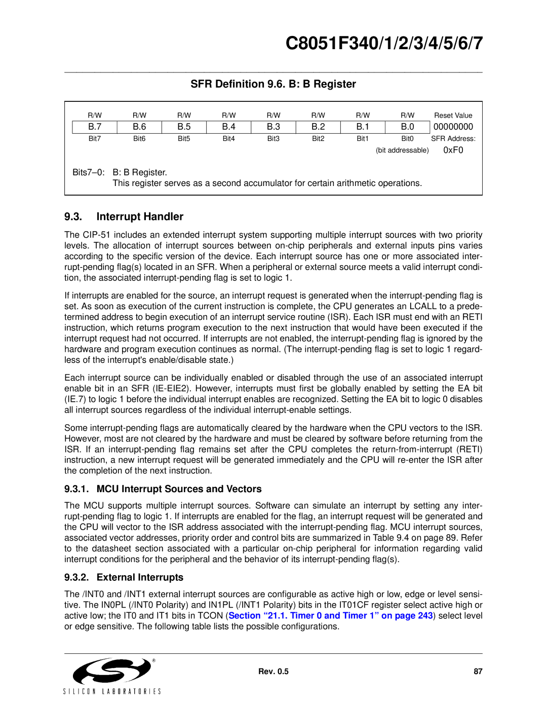
SFR Definition 9.6. B: B Register
| R/W |
| R/W | R/W | R/W | R/W | R/W | R/W |
| R/W | Reset Value | |
| B.7 |
| B.6 |
| B.5 | B.4 | B.3 | B.2 | B.1 |
| B.0 | 00000000 |
| Bit7 |
| Bit6 | Bit5 | Bit4 | Bit3 | Bit2 | Bit1 |
| Bit0 | SFR Address: | |
|
|
|
|
|
|
|
|
|
| (bit addressable) | 0xF0 | |
| B: B Register. |
|
|
|
|
|
|
|
| |||
|
| This register serves as a second accumulator for certain arithmetic operations. |
| |||||||||
|
|
|
|
|
|
|
|
|
|
|
|
|
9.3.Interrupt Handler
The
If interrupts are enabled for the source, an interrupt request is generated when the
Each interrupt source can be individually enabled or disabled through the use of an associated interrupt enable bit in an SFR
Some
9.3.1. MCU Interrupt Sources and Vectors
The MCU supports multiple interrupt sources. Software can simulate an interrupt by setting any inter-
9.3.2. External Interrupts
The /INT0 and /INT1 external interrupt sources are configurable as active high or low, edge or level sensi- tive. The IN0PL (/INT0 Polarity) and IN1PL (/INT1 Polarity) bits in the IT01CF register select active high or active low; the IT0 and IT1 bits in TCON (Section “21.1. Timer 0 and Timer 1” on page 243) select level or edge sensitive. The following table lists the possible configurations.
Rev. 0.5 | 87 |