Silicon Laboratories C8051F341, C8051F347 Serial Clock Timing, Master Mode Data/Clock Timing

Models: C8051F346 C8051F347 C8051F344 C8051F342 C8051F343 C8051F345 C8051F340 C8051F341

1 282
Download 282 pages 2.89 Kb
Page 234
Image 234

C8051F340/1/2/3/4/5/6/7

20.5. Serial Clock Timing

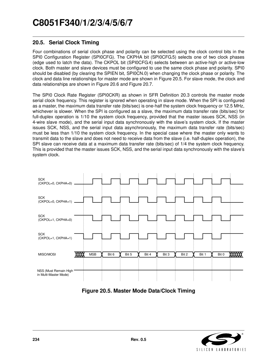
Four combinations of serial clock phase and polarity can be selected using the clock control bits in the SPI0 Configuration Register (SPI0CFG). The CKPHA bit (SPI0CFG.5) selects one of two clock phases (edge used to latch the data). The CKPOL bit (SPI0CFG.4) selects between an active-high or active-low clock. Both master and slave devices must be configured to use the same clock phase and polarity. SPI0 should be disabled (by clearing the SPIEN bit, SPI0CN.0) when changing the clock phase or polarity. The clock and data line relationships for master mode are shown in Figure 20.5. For slave mode, the clock and data relationships are shown in Figure 20.6 and Figure 20.7.

The SPI0 Clock Rate Register (SPI0CKR) as shown in SFR Definition 20.3 controls the master mode serial clock frequency. This register is ignored when operating in slave mode. When the SPI is configured as a master, the maximum data transfer rate (bits/sec) is one-half the system clock frequency or 12.5 MHz, whichever is slower. When the SPI is configured as a slave, the maximum data transfer rate (bits/sec) for full-duplex operation is 1/10 the system clock frequency, provided that the master issues SCK, NSS (in 4-wire slave mode), and the serial input data synchronously with the slave’s system clock. If the master issues SCK, NSS, and the serial input data asynchronously, the maximum data transfer rate (bits/sec) must be less than 1/10 the system clock frequency. In the special case where the master only wants to transmit data to the slave and does not need to receive data from the slave (i.e. half-duplex operation), the SPI slave can receive data at a maximum data transfer rate (bits/sec) of 1/4 the system clock frequency. This is provided that the master issues SCK, NSS, and the serial input data synchronously with the slave’s system clock.

SCK

(CKPOL=0, CKPHA=0)

SCK

(CKPOL=0, CKPHA=1)

SCK

(CKPOL=1, CKPHA=0)

SCK

(CKPOL=1, CKPHA=1)

MISO/MOSI

MSB

Bit 6

Bit 5

Bit 4

Bit 3

Bit 2

Bit 1

Bit 0

NSS (Must Remain High

in Multi-Master Mode)

Figure 20.5. Master Mode Data/Clock Timing

234

Rev. 0.5

Page 234
Image 234
Silicon Laboratories C8051F341, C8051F347, C8051F346, C8051F343, C8051F340 Serial Clock Timing, Master Mode Data/Clock Timing