Silicon Laboratories C8051F341 Programmable Digital I/O and Crossbar, Digital Crossbar Diagram

Models: C8051F346 C8051F347 C8051F344 C8051F342 C8051F343 C8051F345 C8051F340 C8051F341

1 282
Download 282 pages 2.89 Kb
Page 26
Image 26

C8051F340/1/2/3/4/5/6/7

1.6.Programmable Digital I/O and Crossbar

C8051F340/1/4/5 devices include 40 I/O pins (five byte-wide Ports); C8051F342/3/6/7 devices include 25 I/O pins (three byte-wide Ports, and a 1-bit-wide Port). The C8051F340/1/2/3/4/5/6/7 Ports behave like typ- ical 8051 Ports with a few enhancements. Each Port pin may be configured as an analog input or a digital I/O pin. Pins selected as digital I/Os may additionally be configured for push-pull or open-drain output. The “weak pull-ups” that are fixed on typical 8051 devices may be globally disabled, providing power savings capabilities.

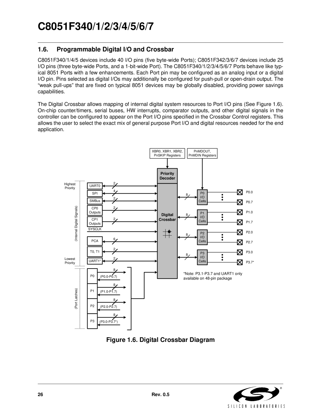
The Digital Crossbar allows mapping of internal digital system resources to Port I/O pins (See Figure 1.6). On-chip counter/timers, serial buses, HW interrupts, comparator outputs, and other digital signals in the controller can be configured to appear on the Port I/O pins specified in the Crossbar Control registers. This allows the user to select the exact mix of general purpose Port I/O and digital resources needed for the end application.

XBR0, XBR1, XBR2,


PnMDOUT,

PnSKIP Registers


PnMDIN Registers


Highest Priority

(Internal Digital Signals)

Lowest Priority

(Port Latches)

2

UART0

4

SPI

2

SMBus

CP0

2

Outputs

2


CP1

Outputs


SYSCLK


6

PCA

2


T0, T1


2


UART1*


8

P0

(P0.0-P0.7)


8

P1

(P1.0-P1.7)


8

P2

(P2.0-P2.7)


8

P3

(P3.0-P3.7*)

Priority

Decoder

Digital

Crossbar

8

P0

P0.0

I/O


Cells

P0.7

8

P1

P1.0

I/O


Cells

P1.7

8

P2

P2.0

I/O


Cells

P2.7

8

P3

P3.0

I/O


Cells

P3.7*

*Note: P3.1-P3.7 and UART1 only available on 48-pin package

Figure 1.6. Digital Crossbar Diagram

26

Rev. 0.5

Page 26
Image 26
Silicon Laboratories C8051F341, C8051F347, C8051F346 Programmable Digital I/O and Crossbar, Digital Crossbar Diagram