C8051F340/1/2/3/4/5/6/7
16.3. USB Register Access
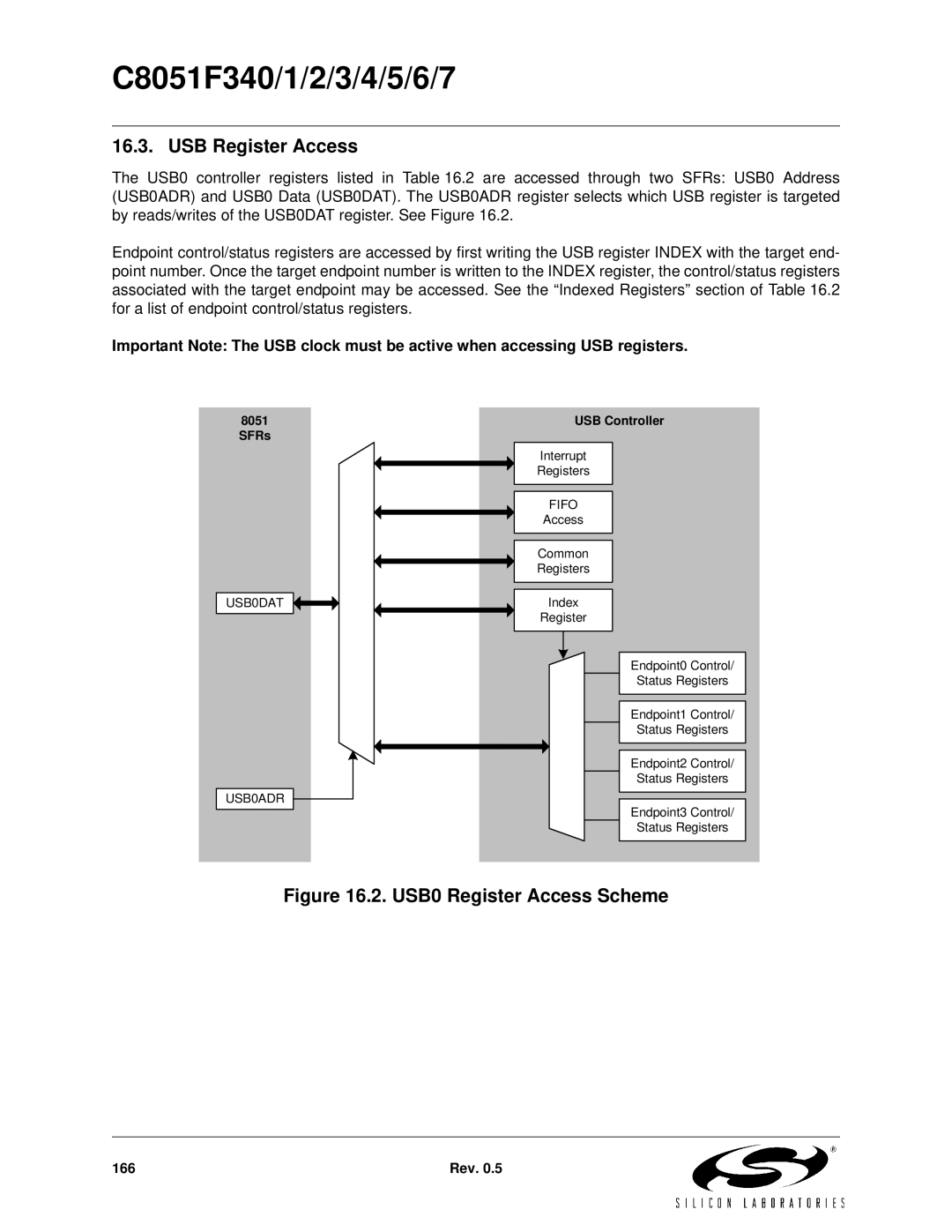
The USB0 controller registers listed in Table 16.2 are accessed through two SFRs: USB0 Address (USB0ADR) and USB0 Data (USB0DAT). The USB0ADR register selects which USB register is targeted by reads/writes of the USB0DAT register. See Figure 16.2.
Endpoint control/status registers are accessed by first writing the USB register INDEX with the target end- point number. Once the target endpoint number is written to the INDEX register, the control/status registers associated with the target endpoint may be accessed. See the “Indexed Registers” section of Table 16.2 for a list of endpoint control/status registers.
Important Note: The USB clock must be active when accessing USB registers.
8051 SFRs
USB0DAT
USB0ADR
USB Controller
Interrupt
Registers
FIFO
Access
Common
Registers
Index
Register
Endpoint0 Control/
Status Registers
Endpoint1 Control/
Status Registers
Endpoint2 Control/
Status Registers
Endpoint3 Control/
Status Registers
Figure 16.2. USB0 Register Access Scheme
166 | Rev. 0.5 |