C8051F340/1/2/3/4/5/6/7
SFR Definition 21.2. TMOD: Timer Mode
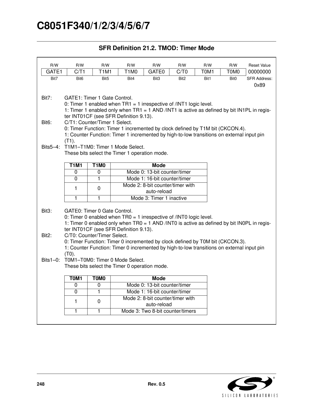
R/W | R/W | R/W | R/W | R/W | R/W | R/W | R/W | Reset Value |
GATE1 | C/T1 | T1M1 | T1M0 | GATE0 | C/T0 | T0M1 | T0M0 |
Bit7 | Bit6 | Bit5 | Bit4 | Bit3 | Bit2 | Bit1 | Bit0 |
00000000
SFR Address:
|
|
|
| 0x89 |
Bit7: | GATE1: Timer 1 Gate Control. | |||
| 0: Timer 1 enabled when TR1 = 1 irrespective of /INT1 logic level. | |||
| 1: Timer 1 enabled only when TR1 = 1 AND /INT1 is active as defined by bit IN1PL in regis- | |||
| ter INT01CF (see SFR Definition 9.13). | |||
Bit6: | C/T1: Counter/Timer 1 Select. | |||
| 0: Timer Function: Timer 1 incremented by clock defined by T1M bit (CKCON.4). | |||
| 1: Counter Function: Timer 1 incremented by | |||
| (T1). |
|
|
|
| These bits select the Timer 1 operation mode. | |||
|
|
|
|
|
| T1M1 | T1M0 | Mode |
|
| 0 | 0 | Mode 0: |
|
| 0 | 1 | Mode 1: |
|
| 1 | 0 | Mode 2: |
|
|
| |||
|
|
|
| |
| 1 | 1 | Mode 3: Timer 1 inactive |
|
Bit3: | GATE0: Timer 0 Gate Control. | |||
0:Timer 0 enabled when TR0 = 1 irrespective of /INT0 logic level.
1:Timer 0 enabled only when TR0 = 1 AND /INT0 is active as defined by bit IN0PL in regis- ter INT01CF (see SFR Definition 9.13).
Bit2: | C/T0: Counter/Timer Select. | |||
| 0: Timer Function: Timer 0 incremented by clock defined by T0M bit (CKCON.3). | |||
| 1: Counter Function: Timer 0 incremented by | |||
| (T0). |
|
|
|
| These bits select the Timer 0 operation mode. | |||
|
|
|
|
|
| T0M1 | T0M0 | Mode |
|
| 0 | 0 | Mode 0: |
|
| 0 | 1 | Mode 1: |
|
| 1 | 0 | Mode 2: |
|
|
| |||
|
|
|
| |
| 1 | 1 | Mode 3: Two |
|
248 | Rev. 0.5 |