Development System Reference Guide
Development System Reference Guide
Guide Contents
About This Guide
Preface About This Guide
Typographical
Additional Resources
Conventions
Allow block blockname
Online Document
Preface About This Guide Convention Meaning or Use Example
Loc1 loc2 ... locn
Table of Contents
Tcl
PARTGen
MAP
Logical Design Rule Check
NGDBuild
Physical Design Rule Check
PAR
Development System Reference Guide
XPower
PIN2UCF
Trace
Trace Output Files
Speedprint
BitGen
BSDLAnno
PROMGen
IBISWriter
TAEngine
CPLDfit
Tsim
Hprep6
NetGen
Development System Reference Guide
Xflow
Data2MEM
EDIF2NGD, and NGDBuild
Introduction
Command Line Program Overview
1Command Line Programs in the Design Flow Design Flow Step
Execute Commands File
Command Line Syntax
Command Line Options
Introduction
Help
Command Line Options
Symbol Description
Programname -harchitecturename
Introduction Symbol Description
Intstyle Integration Style
Programname -h filename
2Part Number Examples Specification
Part Number
Invoking Command Line Programs
Introduction 2Part Number Examples Specification
Design Flow
Design Flow Overview
Design Flow
Xilinx Design Flow
Design Flow Overview
2Xilinx Software Design Flow FPGAs
3Xilinx Software Design Flow CPLDs
Design Entry and Synthesis
Design Entry and Synthesis
Hierarchical Design
Core Generator Tool FPGAs Only
Schematic Entry Overview
Library Elements
Constraints
HDL Entry and Synthesis
Functional Simulation
Mapping Constraints FPGAs Only
Design Implementation
Block Placement
Timing Specifications
Netlist Translation Programs
Design Implementation
5Design Implementation Flow FPGAs
6Design Implementation Flow CPLDs
Bitstream Generation FPGAs Only
Mapping FPGAs Only
Placing and Routing FPGAs Only
Design Verification
1Verification Tools Verification Type
Design Verification
7Three Verification Methods of the Design Flow FPGAs
Simulation
Back-Annotation
9Back-Annotation Flow for FPGAs
Schematic-Based Simulation
NetGen
HDL-Based Simulation
Timing Simulation
11Simulation Points for HDL Designs
2Five Simulation Points in HDL Design Flow UniSim SimPrim
Static Timing Analysis FPGAs Only
Xilinx Design Download Cables
In-Circuit Verification
Design Rule Checker FPGAs Only
Probe
Design Size and Performance
3Global Clock Resources Fpga Family Number Destination Pins
Fpga Design Tips
Global Clock Distribution
Data Feedback and Clock Enable
12 Gated Clock
13Synchronous Design Using Data Feedback
Counters
Q0. . . .Q7Q8. . . .Q15
Other Synchronous Design Considerations
Q0. . . .Q7 Q8. . . .Q15
Tcl
Tcl Overview
Accessing Help
Xilinx Tcl Shell
Tcl Fundamentals
Tcl Fundamentals
Xilinx Namespace
Xilinx Tcl Commands
1Xilinx Tcl Commands for General Usage Subcommands
Project create and manage projects
Partition support design preservation
Tcl Commands for General Usage
2Xilinx Tcl Commands for Advanced Scripting Subcommands
Get get partition properties
Tcl Commands for General Usage
Delete delete a partition
Partition delete /stopwatch/Instdcm1
Partition new /stopwatch/Instdcm1
New create a new partition
Partition get /stopwatch/Instdcm1 preserve
Partition properties
Properties list available partition properties
Rerun force partition synthesis and implementation
Set set partition preserve property
4Process Tasks
Process run and manage project processes
Run run process task
Project create and manage projects
Clean remove system-generated project files
Project clean
Getprocesses get project processes
Close close the ISE project
Get get project properties
Project close
Project getprocesses -instance Instdcm1
New create a new ISE project
Open open an ISE project
Project new watchver.ise
Project properties -process all
Properties list project properties
Set set project properties, values, and options
Project set Map Effort Level high
Set device set device
Set family set device family
Project set device xc2vp2
Project set family Virtex2p
Set package set device package
Set speed set device speed
Project set package fg256
Delete delete timing analysis
Timinganalysis generate timing analysis reports
Set top set the top-level module/entity
Project set speed
Disableconstraints disable timing constraints
Disablecpt disable components for path tracing control
Stopwatchtiming TSclk=PERIOD TIMEGROUP\sclk\
Enablecpt enable components for path tracing control
Timinganalysis enableconstraints
Ns High 50.00000%
Regsrclk ureg1 ureg2 ureg3
Timinganalysis enablecpt stopwatchtiming
Get get analysis property
Ascii
New new timing analysis
Run run analysis
Reset reset path filters and constraints
Timinganalysis reset stopwatchtiming
Saveas save analysis report
Timinganalysis set stopwatchtiming
Set set analysis properties
Setconstraint set constraint for custom analysis
Analysisspeed
Period 13 sclk
Setendpoints set source and destination endpoints
Timinganalysis setconstraint stopwatchtiming
Timinganalysis setfilter stopwatchtiming nets
Setquery set up net or timegroup report
Setfilter set filter for analysis
Exclude uregnet1 uregnet2 uregnet3
Add add file to project
Showsettings generate settings report
Xfile manage project files
Example
Xfile add *.vhd /mysource/mysubdir timing.ucf
Get get project file properties
Remove remove file from project
Xfile get timestamp stopwatch.vhd
Appendto add objects to a collection
Tcl Commands for Advanced Scripting
Collection create and manage a collection
Xfile remove stopwatch.vhd
Set colVar1 search * -type instance
Tcl Commands for Advanced Scripting
Copy copy a collection
Set colVar2 $colVar1
Set colVar2 search /top/T* -type instance
Equal compare two collections
Set colVar2 collection copy $colVar1
Collection equal $colVar1 $colVar2
Foreach iterate over elements in a collection
Get get collection property
Set item collection index $colVar
Index extract a collection object
Properties list available collection properties
Object name $item
Collection properties
Removefrom remove objects from a collection
Set set the property for all collections
Collection set displaytype true
Object get object information
Sizeof show the number of objects in a collection
Collection sizeof $colVar
Collection foreach obj $colVar set objProps
Get get object properties
Name name of the object
Object properties $obj foreach prop $objProps
Set colVar search * -type partition
Properties list object properties
Object name collection index $colVar
Object type collection index $colVar
Search search and return matching objects
Type type of object
6Project Properties Property Name Description
Project Properties and Options
Search /stopwatch -type instance
Option Name Synthesis Tool
Project Properties and Options
NGDBuild Options Option Name Implementation Tool
Option Name Implementation Tool
Tcl 10 PAR Options
Example Tcl Scripts
Example Tcl Scripts
Sample Tcl Script for General Usage
Tcl
Sample Tcl Script for Advanced Scripting
100
PARTGen Syntax
PARTGen
PARTGen Overview
Partgen options
PARTGen Options
PARTGen Input Files
PARTGen Output Files
Arch Print Information for Specified Architecture
PARTGen Options
Print a List of Devices, Packages, and Speeds
PARTGen Options
2s400e
Pname
Creates Package file and Partlist Files
Nopkgfile No Package File
Xcv400 Device V400bg432 Part
Partlist File
Creates Package and Partlist Files
Partlist File
Header
Device Attributes
Part architecture family partname diename packagefilename
Select RAM
PKG File
PKG File
Done
Logical Design Rule Check
Logical DRC Overview
Net Check
Logical DRC Checks
Block Check
Pad Check
Logical DRC Checks
Clock Buffer Check
Name Check
1Checked Primitive Pins NGD Primitive Pins Checked
Primitive Pin Check
NGDBuild
NGDBuild Overview
Converting a Netlist to an NGD File
1NGDBuild Design Flow
NGDBuild Syntax
NGDBuild Syntax
NGDBuild Input Files
Ngdbuild options designname ngdfile.ngd
120
NGDBuild Intermediate Files
Add PADs to Top-Level Port Signals
NGDBuild Output Files
NGDBuild Options
Dd Destination Directory
Aul Allow Unmatched LOCs
Bm Specify BMM Files
Ignore UCF File
NGDBuild Options
Insertkeephierarchy
Libraries to Search
Synopsys
Modular assemble -pimpath pimdirectorypath
Modular assemble Module Assembly
Modular initial Initial Budgeting of Modular Design
Usepimmodulename1 -usepimmodulename2
Modular module -active modulename
Modular module Active Module Implementation
Nt Netlist Translation Type
Pimcreate pimdirectory -ncd designnamerouted.ncd
Allow Unexpanded Blocks
Ignore LOC Constraints
Sd Search Specified Directory
Verbose Report All Messages
Uc User Constraints File
Ur Read User Rules File
Uc ucffile.ucf
128
MAP
MAP Overview
MAP Syntax
Map options infile.ngd pcffile.pcf
MAP Input Files
MAP Input Files
MAP Output Files
MAP Options
1Map Options and Architectures
MAP Options 1Map Options and Architectures
Bp Map Slice Logic
Pack CLBs
Cpackfactor
Equivalentregisterremoval Remove Redundant Registers
Cm Cover Mode
Detail Write Out Detailed MAP Report
Cm area speed balanced
Gf Guide NCD File
Gm Guide Mode
Gm incremental Guide Mode incremental
Globalopt Global Optimization
Ise ISE Project File
Ignorekeephierarchy Ignore Keephierarchy Properties
Ir Do Not Use RLOCs to Generate RPMs
Map to Input Functions
No logic replication
Output File Name
Ol Overall Effort Level
Olstdmedhigh
Registerduplication Duplicate Registers
Pr Pack Registers in I/O
No Register Ordering
Retiming Register Retiming During Global Optimization
Tx on off aggressive limit
Timing Timing-Driven Packing and Placement
Tx Transform Buses
Xe Extra Effort Level
MAP Process
Do Not Remove Unused Logic
MAP Process
Register Ordering
Register Ordering
Data01 Addr02 Atod03 Dtoa04
Guided Mapping
3Guided Mapping
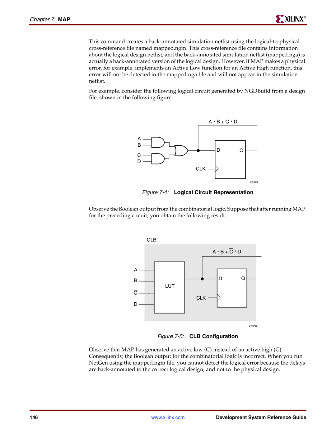
Simulating Map Results
Simulating Map Results
4Logical Circuit Representation
MAP Report MRP File
MAP Report MRP File
148
Development System Reference Guide 149
Type Block GND Xstgnd
IOB
152
Halting MAP
Halting MAP
154
Physical Design Rule Check
DRC Overview
DRC Output File
DRC Syntax
DRC Input File
DRC Options
DRC Checks
DRC Checks
Report Incomplete Programming
DRC Errors and Warnings
PAR
Place and Route Overview
PAR Flow
Routing
PAR Process
Placing
Timing-driven PAR
Par -k previous.ncd reentrant.ncd pref.pcf
Command Line Examples
Par input.ncd output.ncd
Guided PAR
Guided PAR
PCI Cores
PAR Output Files
PAR Syntax
PAR Input Files
PAR Syntax
PAR Options
1Effort Level Options Function Range Default
General Options Function Range Default
Ol value for the router
Existingfile
PAR Options 2General Options Function Range Default
Guide Options Function Range Default
Gf Guide NCD File
Execute Commands File
Detailed Listing of Options
Re-Entrant Routing
Gm Guide Mode
Intstyle Integration Style
PAR Options
Nopad No Pad
Multi-Tasking Mode
Number of PAR Iterations
Ol Overall Effort Level
Pl Placer Effort Level
No Placement
Power Power Aware PAR
No Routing
Ub Use Bonded I/Os
Number of Results to Save
Starting Placer Cost Table
Overwrite Existing Files
Xe Extra Effort Level
Performance Evaluation Mode
PAR Reports
PAR Reports
Place and Route Report File
Development System Reference Guide 175
Ing score in parenthesis
Development System Reference Guide 177
Par -n 3 -pl high -rl std address.ncd output.dir
Multi Pass Place and Route Mppr
Placer effort levelrouter effort levelcost table number
Guide Reporting
Select I/O Utilization and Usage Summary
Importing the PAD File Information
Multi Pass Place and Route Mppr
Best Performance Mode
Xplorer
Xplorer
Timing Closure Mode
Xplorer Syntax
Xplorer Options
Xplorer Input Files
Xplorer Output Files
5Xplorer Options Function
Xplorer Report
Xplorer 5Xplorer Options Function
184
ReportGen Input Files
ReportGen
ReportGen Syntax
ReportGen Output Files
Isexflowsilent
ReportGen Options
Option Usage Function
Padfmt padcsvtxt
Turns Engine PAR Multi-Tasking Option
Turns Engine PAR Multi-Tasking Option
Turns Engine Overview
Par -m nodefilename -ol high -n 10 mydesign.ncd output.dir
Turns Engine Syntax
Turns Engine Input Files
System Requirements
Turns Engine Output Files
Limitations
Turns Engine Environment Variables
Debugging
Rsh machinename
Screen Output
Node Status JOB Time
Halting PAR
Halting PAR
196
XPower
XPower Overview
Fpga Designs
XPower Syntax
Files Used by XPower
Cpld Designs
VCD Data Entry
Using XPower
Using XPower
Limit
Rename Power Report
Other Methods of Data Entry
Ls List Supported Devices
Tb Turn On Time Based Reporting
Specify Settings XML Input File
Specify VCD file
Wx Write XML File
Standard Reports
Command Line Examples
Power Reports
Advanced Reports
Power Reports
Detailed Reports
204
PIN2UCF
PIN2UCF Overview
PIN2UCF Flow
PIN2UCF Output Files
PIN2UCF Syntax
PIN2UCF Input Files
PIN2UCF Syntax
Write to a Report File
PIN2UCF Options
PIN2UCF Scenarios
Outfile.ucf
Existing Pinlock section.
210
Trace
Trace Overview
Trce options design.ncd constraint.pcf
Trace Syntax
Trace Input Files
Trce -runmacro.xtm design.ncd constraint.pcf
Trace Output Files
Trace Output Files
Input files to Trace
Advanced Analysis
Generate an Error Report
Trace Options
Fastpaths Report Fastest Paths
Output Timing Report File Name
Nodatasheet No Data Sheet
Limit Timing Report
Trace Options
Skew Analyze Clock Skew for All Clocks
Run Run Timing Analyzer Macro
Change Speed
Skew
Stampstampfile design.ncd
Stamp Generates Stamp timing model files
Report Uncovered Paths
Ulimit
Xml XML Output File Name
Trace Command Line Examples
Generate a Verbose Report
Vlimit
Trace Reports
Trace Reports
Timing Verification with Trace
Net Delay Constraints
Path Delay Constraints
Net Skew Constraints
Clock Skew and Setup Checking
1Path Delay Constraint Terminology Definition
2Clock Skew and Setup Checking Terminology Terms Definition
2Clock Skew Example
3Clock Passing Through Multiple Buffers
Reporting with Trace
5Error reporting for failed timing constraints
Data Sheet Report
Development System Reference Guide 227
BSLOT0 D0S
Guaranteed Setup and Hold Reporting
Report Legend
Setup Times
Hold Times
Summary Report Without a Physical Constraints File Specified
Trce -o summary.twr ramb16s1.ncd
Trce -o summary1.twr ramb16s1.ncd clkperiod.pcf
Development System Reference Guide 233
Trce -e 3 ramb16s1.ncd clkperiod.pcf -o errorreport.twr
Development System Reference Guide 235
236
Development System Reference Guide 237
BUFGMUX.I0
Offset Constraints
Offset Constraints
Offset in Path Details
Offset in Constraint Examples
Offset in Header
Offset in Detailed Path Data
Offset In with Phase Shifted Clock
Offset in Detail Path Clock Path
Development System Reference Guide 243
Offset OUT Constraint Examples
Offset OUT Header
Offset OUT Path Details
Offset OUT Detail Clock Path
Offset OUT Detail Path Data
Period Header
Period Constraints
Period Constraints Examples
Period Constraints
Period Path
Period Path Details
Period Constraint with Phase
Period Path with Phase
Halting Trace
Minimum Period Statistics
Speedprint
Speedprint Overview
Speedprint Options
Specify Temperature
Speedprint Syntax
Min Display Minimum Speed Data
Command Description
Speedprint Example Commands
Speedprint Example Commands
Speedprint Example Reports
Lvttl Fast
BitGen
BitGen Overview
Loutfilename.ll Moutfilename.msk Boutfilename.rbt
BitGen Syntax
Option Output File
BitGen Input Files
BitGen Input Files
BitGen Output Files
BitGen Options
Create Rawbits File
Bitgen -goptionsetting design.ncd design.bit design.pcf
Bd Update Block Rams
Set Configuration
Do Not Run DRC
Binary
ActiveReconfig
ActivateGCLK
CclkPin
ConfigRate
Compress
DebugBitstream
DCIUpdateMode
DCMShutdown
DonePin
DisableBandgap
DONEcycle
DonePipe
Gclkdel0, Gclkdel1, Gclkdel2, Gclkdel3
DriveDone
Encrypt
GSRcycle
HswapenPin
GWEcycle
GTScycle
Key0, Key1, Key2, Key3, Key4, Key5
LCKcycle
KeyFile
Keyseq0, Keyseq1, Keyseq2, Keyseq3, Keyseq4, Keyseq5
M0Pin
Matchcycle
M1Pin
M2Pin
PartialGCLK
PartialRight
PartialMask0, PartialMask1, PartialMask2
PartialLeft
Persist
ReadBack
PowerdownPin
ProgPin
Security
StartKey
SEURepair
StartCBC
StartupClk
TdoPin
TckPin
TdiPin
TmsPin
UserID
No BIT File
UnusedPin
Create a Partial Bit File
Create a Logic Allocation File
Generate a Mask File
Overwrite Existing Output File
276
BSDLAnno
BSDLAnno Overview
BSDLAnno Output Files
BSDLAnno Syntax
BSDLAnno Input Files
BSDLAnno Options
Generic Parameter
BSDLAnno File Composition
Entity Declaration
BSDLAnno File Composition
Logical Port Description
Package Pin-Mapping
TAP Description
USE Statement
Scan Port Identification
Bsdl File Modifications for Single-Ended Pins
Boundary Register Description
Explanation
Header Comments
Boundary Scan Behavior in Xilinx Devices
Modifications to the Designwarning Section
BSDLAnno BSDLAnno version number
PROMGen
PROMGen Overview
PROMGen Output Files
PROMGen Syntax
PROMGen Input Files
Promgen options
PROMGen Options
Load Prom File
Add BIT FIles
Prom Format
File1.bit file2.bit
Load Upward
Prom Size
Template File
Ver Version
Enable Compression
Bit Swapping in Prom Files
PROMGen Examples
PROMGen Examples
292
IBISWriter
IBISWriter Overview
IBISWriter Syntax
Ibiswriter options infile outfile.ibs
IBISWriter Options
IBISWriter Input Files
IBISWriter Output Files
Set Reference Voltage
Ml Multilingual Support
Architecture Option Value Description
Pin Generate Package Parasitics
IBISWriter Options
298
CPLDfit
CPLDfit Overview
CPLDfit Output Files
CPLDfit Syntax
CPLDfit Input Files
CPLDfit Options
Keepio Prevent Optimization of Unused Inputs
Inputs Number of Inputs to Use During Optimization
Iostd Specify I/O Standard
Loc Keep Specified Location Constraints
Nogsropt Disable Global Set/Reset Optimization
Nofbnand Disable Use of Foldback Nands
Nogclkopt Disable Global Clock Optimization
Nogtsopt Disable Global Output-Enable Optimization
Specify Xilinx Part
Power Set Power Mode
Optimize Optimize Logic for Density or Speed
Pinfbk Use Pin Feedback
Slew Set Slew Rate
Terminate Set to Termination Mode
Unused Set Termination Mode of Unused I/Os
Wysiwyg Do Not Perform Optimization
306
Tsim
Tsim Syntax
Tsim Input Files
TAEngine
TAEngine Overview
TAEngine Syntax
1TAEngine Design Flow
Iopath Trace Paths
TAEngine Options
Detail Detail Report
Specify Output Filename
312
Hprep6
1Hprep6 Design Flow
Autosig Automatically Generate Signature
Hprep6 Syntax
Hprep6 Options
Produce ISC File
Nopullup Disable Pullups
Specify Signature Value for Readback
Tmv Specify Test Vector File
316
NetGen
NetGen Overview
NetGen
1NetGen Output File Types Input Design File
NetGen Supported Flows
NetGen Simulation Flow
NetGen Functional Simulation Flow
NetGen Simulation Flow
Output files for NetGen Functional Simulation
NetGen Timing Simulation Flow
Syntax for NetGen Functional Simulation
Ngcbuildoptions toplevelnetlistfile outputngcfile
NetGen Timing Simulation Flow
Syntax for NetGen Timing Simulation
Fpga Timing Simulation
Input files for Cpld Timing Simulation
Output files for Fpga Timing Simulation
Cpld Timing Simulation
Output files for Cpld Timing Simulation
Options for NetGen Simulation Flow
Module Simulation of Active Module
Insertppbuffers Insert Path Pulse Buffers
Mhf Multiple Hierarchical Files
Change Speed
Ofmt Output Format
Pcf PCF File
Sim Generate Simulation Netlist
Tp Bring Out Global 3-State Net as Port
Ti Top Instance Name
Tm Top Module Name
Insertglbl Insert glbl.v Module
Sdfanno Include $sdfannotate
Ne No Name Escaping
Pf Generate PIN File
Sdfpath Full Path to SDF File
VHDL-Specific Options for Functional and Timing Simulation
NetGen Equivalence Checking Flow
NetGen Equivalence Checking Flow
Xon Select Output Behavior for Timing Violations
Xon truefalse
Syntax for NetGen Equivalence Checking
Input files for NetGen Equivalence Checking
Ecn Equivalence Checking
Output files for NetGen Equivalence Checking
Options for NetGen Equivalence Checking Flow
Module Verification of Active Module
NetGen Static Timing Analysis Flow
NetGen Static Timing Analysis Flow
Ngm Design Correlation File
Syntax for NetGen Static Timing Analysis
Input files for Static Timing Analysis
Output files for Static Timing Analysis
Options for NetGen Static Timing Analysis Flow
336
Preserving and Writing Hierarchy Files
Preserving and Writing Hierarchy Files
Sta Generate Static Timing Analysis Netlist
Modulename .sim Modulename .ecn Modulename .sta
Hierarchy Information File
Dedicated Global Signals in Back-Annotation Simulation
Testbench File
Dedicated Global Signals in Back-Annotation Simulation
Global Signals in Verilog Netlist
Global Signals in Vhdl Netlist
340
Xflow
Xflow Overview
Xflow Syntax
1XFLOW Design Flow
Xflow Input Files
Xflow Input Files
Xflow Output Files
Xflow Output Files
1XFLOW Output Files FPGAs and CPLDs
2XFLOW Output Files FPGAs
Xflow Flow Types
Assemble Module Assembly
Xflow Flow Types
3XFLOW Output Files CPLDs
Ecn Create a File for Equivalence Checking
Config Create a BIT File for FPGAs
Configoptionfile
4Option Files for -assemble Flow Type Description
5Option Files for -ecn Flow Type Description
Fit Fit a Cpld
Fsim Create a File for Functional Simulation
6Option Files for -fit Flow Type Description
Xflow -p xc2v250fg256-5 -fsim genericverilog.opt testclk.v
Implement Implement an Fpga
7Option Files for -fsim Flow Type
Implement optionfile
Initial budget.opt
Initial Initial Budgeting of Modular Design
Xflow Flow Types 8Option Files for -implement Flow Type
Xflow -p xc2v250fg256-5 -initial budget.opt top.edf
9Option Files for -module Flow Type
Module Active Module Implementation
Moduleoptionfile -activemodulename
10Option Files for -mppr Flow Type Description
Mppr Multi-Pass Place and Route for FPGAs
Sta Create a File for Static Timing Analysis
11Option Files for -sta Flow Type Description
Synthoptionfile
Synth
Synthesis Types
12Option Files for -synth Flow Type Description
Tsim Create a File for Timing Simulation
Option Files for -synth Flow Types
Testclk.prj
Flow Files
13Option Files for -tsim Flow Type Description
Flow File Format
Fpga
Exports
Flag Enabled Disabled
Triggers
Reports
User Command Blocks
End Program programname
Xflow Option Files
Option File Format
Ed Copy Files to Export Directory
Xflow Options
Active Active Module
Specify a Global Variable
Ooutputfilename
Norun Creates a Script File Only
Change Output File Name
Xflow -implement balanced.opt -o newname testclk.edf
Pdpimdirectory
Pd PIMs Directory
Rd Copy Report Files
Rdreportdirectory
Wd Specify a Working Directory
Using Xflow Flow Types in Combination
Running Xflow
Running Smart Flow
Running Xflow
Using the SCR, BAT, or TCL File
Using the Xilxflowpath Environment Variable
366
Data2MEM
Data2MEM Overview
Block RAM Memory Map .bmm files
Data2MEM Syntax
Data2MEM Input and Output Files
Executable and Linkable Format .elf files
Bit .bit files
Debugging Information Format Dwarf .drf files
Memory .mem files
Verilog .v files
Vhdl .vhd files
1Data2MEM Command Line Options Description
Data2MEM Options
UCF .ucf files
Data2MEM Options 1Data2MEM Command Line Options
Pp filename
Xilinx Development System Files
Name Type Produced By Description
Appendix
MOD Ascii Trace
NKY
TCL Ascii
378
EDIF2NGD, and NGDBuild
EDIF2NGD
EDIF2NGD Design Flow
EDIF2NGD Output Files
EDIF2NGD Syntax
EDIF2NGD Input Files
Edif2ngd options ediffile ngofile
Aul Allow Unmatched LOCs
Add PADs to Top-Level Port Signals
EDIF2NGD Options
Ignore LOC Constraints
Libraries to Search
Part Number
Llibname
NGDBuild
NGDBuild and the Netlist Readers
NGDBuild
Bus Naming Conventions
Netlist Launcher Netlister
Bus Matching
Busnameindex DI3
Netlist Launcher Netlister
User Rules and System Rules
Netlist Launcher Rules Files
User Rules File
User Rules Format
Development System Reference Guide 389
System Rules File
Value Types in Key Statements
Rules File Examples
Example 1 Edfrule System Rule
Example 2 User Rule
Example 3 User Rule
NGDBuild File Names and Locations
NGDBuild File Names and Locations
Example 4 User Rule
394
Glossary
Abel
Asic
Bonded
Bitstream
Block
Boundary scan
Buft
CAE
CLB
Cmos
Combinatorial logic
Configuration
Contention
Compiler
Dangling bus
Cpld
Daisy chain
Dangling net
DRC
DSP
EDA
Edif
Fifo
Eprom
Fdsd
Fmap
Fpga
Global buffers
Global Set/Reset net
Gate array
Global 3-state net
HDL
Ibuf
Ieee
IFD
Jedec
LSB
MSB
NCD
NGM
PAL
PIM
PLD
Prom
RAM
RTL
ROM
RPM
Signal
SDF standard delay format
Set/reset
Startup symbol
TCL
Trace
Tsim
TTL
Vital
Wire
Vhdl
Xtclsh
422