R
Chapter 6: The Ten-Bit Interface
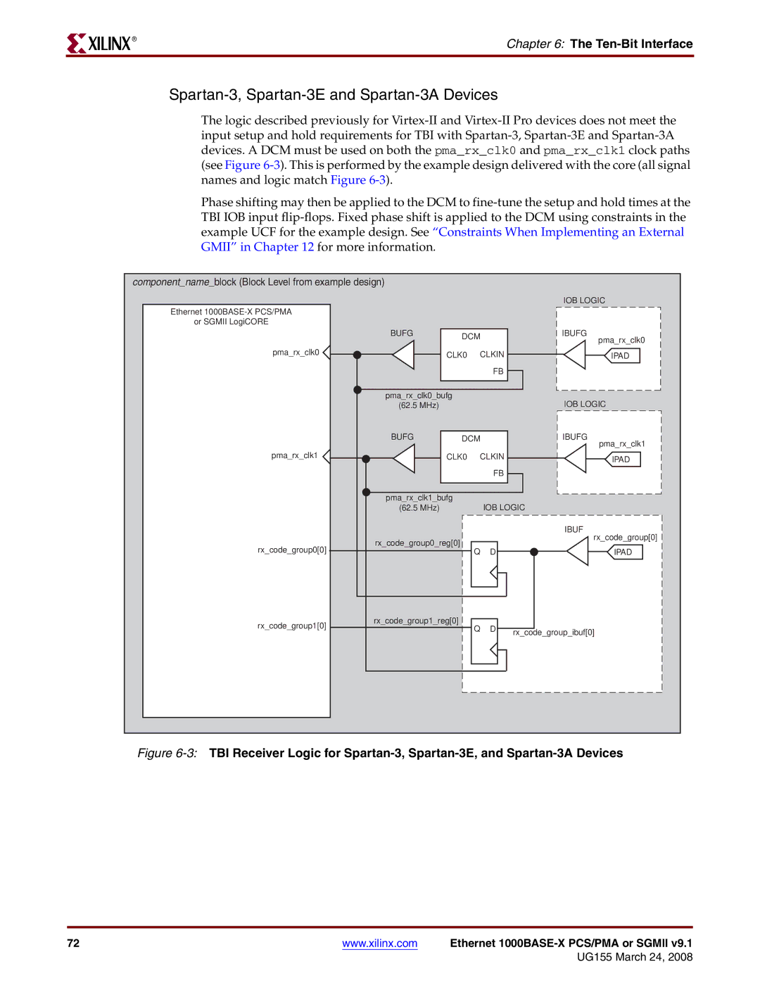
Spartan-3, Spartan-3E and Spartan-3A Devices
The logic described previously for
Phase shifting may then be applied to the DCM to
component_name_block (Block Level from example design)
IOB LOGIC
Ethernet |
|
|
|
|
| |
or SGMII LogiCORE |
|
|
|
|
| |
| BUFG | DCM |
| IBUFG | ||
|
|
| pma_rx_clk0 | |||
|
|
|
|
| ||
pma_rx_clk0 |
| CLK0 | CLKIN | IPAD | ||
|
|
|
| FB |
| |
| pma_rx_clk0_bufg |
|
| IOB LOGIC | ||
| (62.5 MHz) |
|
|
| ||
| BUFG | DCM |
| IBUFG | ||
|
|
|
|
| pma_rx_clk1 | |
pma_rx_clk1 |
| CLK0 | CLKIN | IPAD | ||
|
|
|
| FB |
| |
| pma_rx_clk1_bufg |
| IOB LOGIC | |||
| (62.5 MHz) |
|
| |||
|
|
|
|
| IBUF | |
| rx_code_group0_reg[0] |
|
| rx_code_group[0] | ||
rx_code_group0[0] | Q | D | IPAD | |||
|
| |||||
rx_code_group1[0] | rx_code_group1_reg[0] | Q | D |
| ||
|
| rx_code_group_ibuf[0] | ||||
|
|
| ||||
|
|
|
|
| ||
Figure 6-3: TBI Receiver Logic for Spartan-3, Spartan-3E, and Spartan-3A Devices
72 | www.xilinx.com | Ethernet |