R
Chapter 12: Constraining the Core
In addition, the example design provides pad locking on the TBI for several families. This is included as a guideline only, and there are no specific I/O location constraints for this core.
TBI Input Setup/Hold Timing
Input TBI Timing Specification
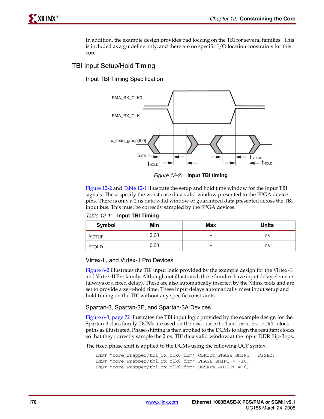
PMA_RX_CLK0
PMA_RX_CLK1
rx_code_group[9:0]
tSETUP
tHOLD
Figure 12-2: Input TBI timing
tSETUP tHOLD
Figure 12-2 and Table 12-1 illustrate the setup and hold time window for the input TBI signals. These specify the worst-case data valid window presented to the FPGA device pins. There is only a 2 ns data valid window of guaranteed data presented across the TBI input bus. This must be correctly sampled by the FPGA devices.
Table 12-1: Input TBI Timing
Symbol | Min | Max | Units |
|
|
|
|
tSETUP | 2.00 | - | ns |
tHOLD | 0.00 | - | ns |
Figure 6-2 illustrates the TBI input logic provided by the example design for the Virtex-II and Virtex-II Pro family. Although not illustrated, these families have input delay elements (always of a fixed delay). These are also automatically inserted by the Xilinx tools and are set to provide a zero-hold time. These input delays automatically meet input setup and hold timing on the TBI without any specific constraints.
Spartan-3, Spartan-3E, and Spartan-3A Devices
Figure 6-3, page 72 illustrates the TBI input logic provided by the example design for the Spartan-3 class family. DCMs are used on the pma_rx_clk0 and pma_rx_clk1 clock paths as illustrated. Phase-shifting is then applied to the DCMs to align the resultant clocks so that they correctly sample the 2 ns. TBI data valid window at the input DDR flip-flops.
The fixed phase shift is applied to the DCMs using the following UCF syntax.
INST "core_wrapper/tbi_rx_clk0_dcm" CLKOUT_PHASE_SHIFT = FIXED;
INST "core_wrapper/tbi_rx_clk0_dcm" PHASE_SHIFT =
INST "core_wrapper/tbi_rx_clk0_dcm" DESKEW_ADJUST = 0;
170 | www.xilinx.com | Ethernet |
|
| UG155 March 24, 2008 |