Ten-Bit-Interface Logic
R
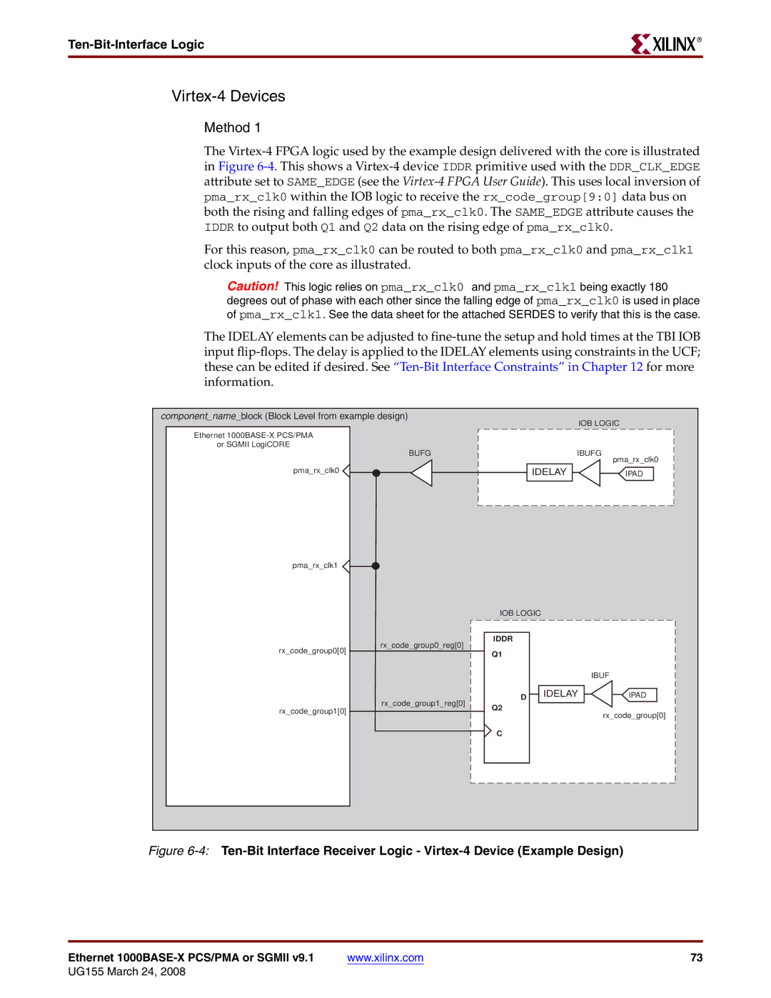
Virtex-4 Devices
Method 1
The
For this reason, pma_rx_clk0 can be routed to both pma_rx_clk0 and pma_rx_clk1 clock inputs of the core as illustrated.
Caution! This logic relies on pma_rx_clk0 and pma_rx_clk1 being exactly 180 degrees out of phase with each other since the falling edge of pma_rx_clk0 is used in place of pma_rx_clk1. See the data sheet for the attached SERDES to verify that this is the case.
The IDELAY elements can be adjusted to
component_name_block (Block Level from example design)
Ethernet
or SGMII LogiCORE
BUFG
pma_rx_clk0
pma_rx_clk1
IOB LOGIC
IBUFG
pma_rx_clk0
IDELAY ![]() IPAD
IPAD
|
| IOB LOGIC | |
| rx_code_group0_reg[0] | IDDR | |
rx_code_group0[0] | Q1 | ||
| |||
|
|
| rx_code_group1_reg[0] | D | IDELAY |
|
| ||
rx_code_group1[0] | Q2 |
| |
|
| ||
|
|
| |
|
| C |
|
IBUF
IPAD
rx_code_group[0]
Figure 6-4: Ten-Bit Interface Receiver Logic - Virtex-4 Device (Example Design)
Ethernet | www.xilinx.com | 73 |