R
Chapter 6: The Ten-Bit Interface
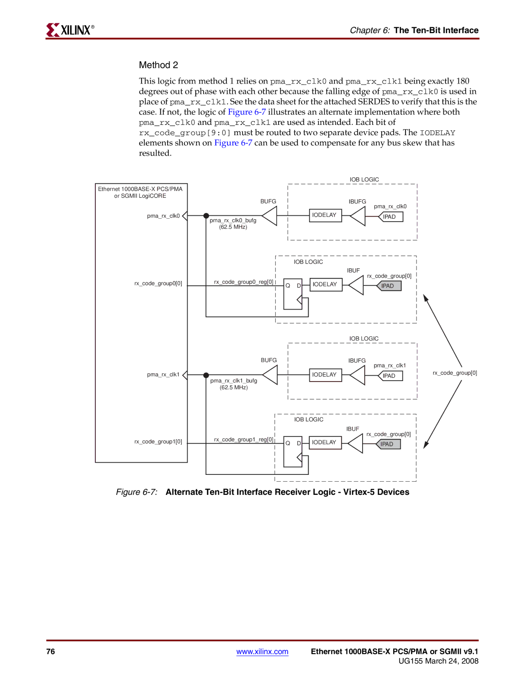
Method 2
This logic from method 1 relies on pma_rx_clk0 and pma_rx_clk1 being exactly 180 degrees out of phase with each other because the falling edge of pma_rx_clk0 is used in place of pma_rx_clk1. See the data sheet for the attached SERDES to verify that this is the case. If not, the logic of Figure
Ethernet
or SGMII LogiCORE
IOB LOGIC
| BUFG | ||||
|
|
|
|
| |
pma_rx_clk0 |
|
|
| IODELAY | |
pma_rx_clk0_bufg | |||||
|
| ||||
| (62.5 MHz) | ||||
|
|
| IOB LOGIC | ||
IBUFG
IBUF
pma_rx_clk0
IPAD
rx_code_group0[0] | rx_code_group0_reg[0] | Q D | IODELAY |
| |||
|
|
|
|
rx_code_group[0]
IPAD
IOB LOGIC
| BUFG | ||||
pma_rx_clk1 |
|
|
|
| |
|
|
| IODELAY | ||
pma_rx_clk1_bufg | |||||
|
| ||||
|
| ||||
| (62.5 MHz) | ||||
|
|
| IOB LOGIC | ||
IBUFG
IBUF
pma_rx_clk1
IPADrx_code_group[0]
rx_code_group1[0] | rx_code_group1_reg[0] | Q D | IODELAY |
| |||
|
|
|
|
rx_code_group[0]
IPAD
Figure 6-7: Alternate Ten-Bit Interface Receiver Logic - Virtex-5 Devices
76 | www.xilinx.com | Ethernet |
|
| UG155 March 24, 2008 |