R
Chapter 12: Constraining the Core
GMII Input Setup/Hold Timing
Input GMII timing specification
GMII_TX_CLK
GMII_TXD[7:0],
GMII_TX_EN,
GMII_TX_ER
tSETUP
tHOLD
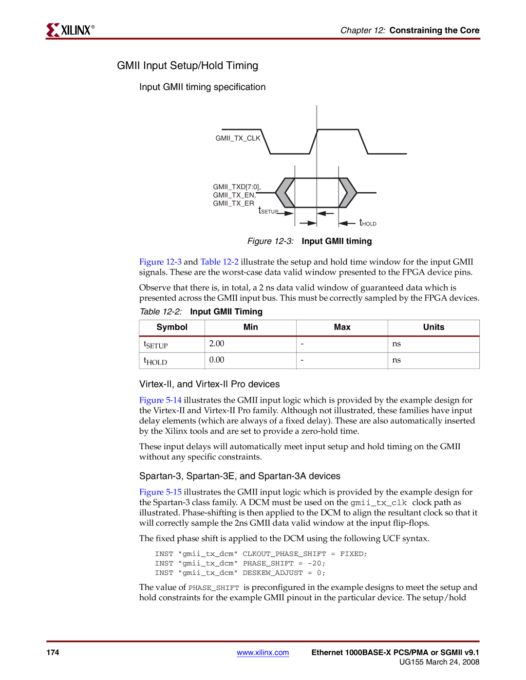
Figure 12-3: Input GMII timing
Figure 12-3 and Table 12-2 illustrate the setup and hold time window for the input GMII signals. These are the worst-case data valid window presented to the FPGA device pins.
Observe that there is, in total, a 2 ns data valid window of guaranteed data which is presented across the GMII input bus. This must be correctly sampled by the FPGA devices.
Table 12-2: Input GMII Timing
Symbol |
| Min |
| Max | Units |
|
|
|
|
|
|
tSETUP | 2.00 |
| - |
| ns |
tHOLD | 0.00 |
| - |
| ns |
Figure 5-14 illustrates the GMII input logic which is provided by the example design for the Virtex-II and Virtex-II Pro family. Although not illustrated, these families have input delay elements (which are always of a fixed delay). These are also automatically inserted by the Xilinx tools and are set to provide a zero-hold time.
These input delays will automatically meet input setup and hold timing on the GMII without any specific constraints.
Spartan-3, Spartan-3E, and Spartan-3A devices
Figure 5-15 illustrates the GMII input logic which is provided by the example design for the Spartan-3 class family. A DCM must be used on the gmii_tx_clk clock path as illustrated. Phase-shifting is then applied to the DCM to align the resultant clock so that it will correctly sample the 2ns GMII data valid window at the input flip-flops.
The fixed phase shift is applied to the DCM using the following UCF syntax.
INST "gmii_tx_dcm" CLKOUT_PHASE_SHIFT = FIXED;
INST "gmii_tx_dcm" PHASE_SHIFT =
INST "gmii_tx_dcm" DESKEW_ADJUST = 0;
The value of PHASE_SHIFT is preconfigured in the example designs to meet the setup and hold constraints for the example GMII pinout in the particular device. The setup/hold
174 | www.xilinx.com | Ethernet |
|
| UG155 March 24, 2008 |