Required Constraints
R
timing which is achieved after
For customers fixing their own pinout, the setup and hold figures reported in the TRCE report can be used to initially setup the approximate DCM phase shift. Appendix C, “Calculating the DCM Fixed Phase Shift Value” describes a more accurate method for fixing the phase shift by using hardware measurement of a unique PCB design.
Virtex-4 devices
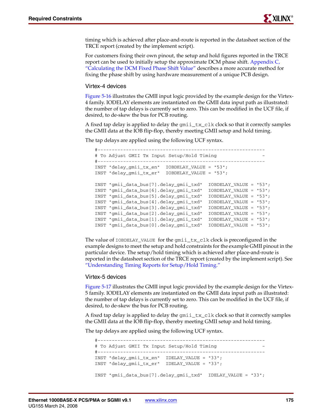
Figure 5-16 illustrates the GMII input logic provided by the example design for the Virtex-
4 family. IODELAY elements are instantiated on the GMII data input path as illustrated: the number of tap delays is currently set to zero. This can be modified in the UCF file, if desired, to de-skew the bus for PCB routing.
A fixed tap delay is applied to delay the gmii_tx_clk clock so that it correctly samples the GMII data at the IOB flip-flop, thereby meeting GMII setup and hold timing.
The tap delays are applied using the following UCF syntax.
# To Adjust GMII Tx Input Setup/Hold Timing | - |
INST "delay_gmii_tx_en" IOBDELAY_VALUE = "53"; |
|
INST "delay_gmii_tx_er" IOBDELAY_VALUE = "53"; |
|
INST "gmii_data_bus[7].delay_gmii_txd" IOBDELAY_VALUE = "53";
INST "gmii_data_bus[6].delay_gmii_txd" IOBDELAY_VALUE = "53";
INST "gmii_data_bus[5].delay_gmii_txd" IOBDELAY_VALUE = "53";
INST "gmii_data_bus[4].delay_gmii_txd" IOBDELAY_VALUE = "53";
INST "gmii_data_bus[3].delay_gmii_txd" IOBDELAY_VALUE = "53";
INST "gmii_data_bus[2].delay_gmii_txd" IOBDELAY_VALUE = "53";
INST "gmii_data_bus[1].delay_gmii_txd" IOBDELAY_VALUE = "53";
INST "gmii_data_bus[0].delay_gmii_txd" IOBDELAY_VALUE = "53";
The value of IOBDELAY_VALUE for the gmii_tx_clk clock is preconfigured in the example designs to meet the setup and hold constraints for the example GMII pinout in the particular device. The setup/hold timing which is achieved after
Virtex-5 devices
Figure 5-17 illustrates the GMII input logic provided by the example design for the Virtex-
5 family. IODELAY elements are instantiated on the GMII data input path as illustrated: the number of tap delays is currently set to zero. This can be modified in the UCF file, if desired, to de-skew the bus for PCB routing.
A fixed tap delay is applied to delay the gmii_tx_clk clock so that it correctly samples the GMII data at the IOB flip-flop, thereby meeting GMII setup and hold timing.
The tap delays are applied using the following UCF syntax.
# To Adjust GMII Tx Input Setup/Hold Timing | - |
INST "delay_gmii_tx_en" IDELAY_VALUE = "33"; |
|
INST "delay_gmii_tx_er" IDELAY_VALUE = "33"; |
|
INST "gmii_data_bus[7].delay_gmii_txd" IDELAY_VALUE = "33";
Ethernet | www.xilinx.com | 175 |