Reference Manual
SC140 DSP Core
SC140 DSP Core Reference Manual
Table of Contents
SC140 DSP Core Reference Manual
Control Registers
SC140 DSP Core Reference Manual
Program Control
Instruction Set Accelerator Plug-In
Programming Rules
Appendix a
SC140 DSP Core Instruction Set
Appendix B
StarCore Registry
Xii
List of Figures
Xiv
List of Tables
Xvi
SC140 DSP Core Reference Manual Xvii
Xviii
List of Examples
SC140 DSP Core Reference Manual
SC140 DSP Core Reference Manual Xxi
Xxii
About This Book
Abbreviations used in this manual are listed below
Abbreviations
Abbreviation Description
ISR
Revision Date Description
Revision History
Target Markets
Chapter Introduction
Architectural Differentiation
Core Architecture Features
Typical System-On-Chip Configuration
SC140 platform
Variable Length Execution Set Vles Software Model
SoC DSP expansion area
System expansion area
Core Architecture Features
Architecture Overview
Chapter Core Architecture
Data Arithmetic Logic Unit Dalu
Block Diagram of the SC140 Core
Bit-Field Unit BFU
Address Generation Unit AGU
Data Register File
Multiply-Accumulate MAC Unit
Bit Mask Unit BMU
Stack Pointer Registers
Memory Interface
Program Sequencer Unit Pseq
Enhanced On-Chip Emulator EOnCE
Instruction Set Accelerator Plug-in Isap Interface
Dalu Architecture
Dalu
Limit EXT
Dalu Programming Model
Data Registers D0-D15
Write to Data Registers
Read from Data Registers
Operand Type Dn.e Dn.h Dn.l
Instruction Description
Data Registers Access Width
Dalu Arithmetic Instructions MAC
Operand Type Data Width Bits
DIV
NEG
Dalu Logical Instructions BFU
Data Shifter/Limiter
Scaling Example
Scaling
Limiting
Calculating the Ln Bit
Scaling Mode Bits Defining the Ln bit Calculation
Limiting with the Moves Instructions
Ln Bit Calculation
10. Scaling and Limiting Interactions
Scaling and Arithmetic Saturation Mode Interactions
Selected Special Six Other Dalu Instructions Mode
Limiting Example
Dalu Arithmetic and Rounding
Data Representation
11. Saturation and Rounding Interactions
Signed Fractional
Data Formats
Signed Integer
12. Two’s Complement Word Representations
Signed Fractional Signed Integer Unsigned Integer
Unsigned Multiplication
Multiplication
Division
Unsigned Arithmetic
Unsigned Comparison
13. Rounding Position in Relation to Scaling Mode
Scaling Mode High Portion Low Portion
Rounding Modes
Convergent Rounding No Scaling
2.6.2 Two’s Complement Rounding
Two’s Complement Rounding No Scaling
14. Arithmetic Saturation Example
Arithmetic Saturation Mode
Fractional Multi-Precision Arithmetic
Multi-Precision Arithmetic Support
Fractional Double-Precision Multiplication
Fractional Mixed-Precision Multiplication
Integer Multi-Precision Arithmetic
10. Signed Integer Double-Precision Multiplication
11. Unsigned Integer Double-Precision Multiplication
Viterbi Decoding Support
AGU Architecture
Address Generation Unit
Address
Arithmetic
Unit AAU
Address Generation Unit
13. AGU Programming Model
AGU Programming Model
Stack Pointer Registers NSP, ESP
Address Registers R0-R15
Shadow Stack Pointer Registers
Offset Registers N0-N3
Base Address Registers B0-B7
Modifier Registers M0-M3
Modifier Control Register Mctl
17. Address Modifier AM Bits
Address Modifier Modes
Addressing Modes
Register Direct Modes
Address Register Indirect Modes
Address Generation Unit
PC Relative Mode
Special Addressing Modes
Memory Access Misalignment
Memory Access Width
20. Addressing Modes Summary
Access Type Aligned Address
Addressing Modes Summary
19. Memory Address Alignment
Address Register Indirect
PC Relative
Special
Address Modifier Modes
Linear Addressing Mode
Reverse-carry Addressing Mode
Modulo Addressing Mode
15. Modulo Addressing Example
Multiple Wrap-Around Modulo Addressing Mode
21. Modulo Register Values for Modulo Addressing Mode
Modifier Mj Address Calculation Arithmetic
23. AGU Arithmetic Instructions
Arithmetic Instructions on Address Registers
Bit Mask Instructions
24. AGU Bit Mask Instructions BMU
Bit Mask Test and Set Semaphore Support Instruction
Label BMTSET.W #mask,R0 JT label
Move Instructions
Semaphore Hardware Implementation
Example of Normal Usage of the Semaphoring Mechanism
MOVE.W
25. AGU Move Instructions
16. Integer Move Instructions
17. Fractional Move Instructions
18. Bit Allocation in MOVE.L D0.eD1.e
Memory Interface
1.1 SC140 Bus Structure
1 SC140 Endian Support
20. Basic Connection between SC140 Core and Memory
Memory Organization
Data Moves
26. Data Representation in Memory
Representation Type Value
22. Data Transfer in Big and Little Endian Modes
Address Data
Multi-Register Moves
Multi-Register Transfer in Big and Little Endian Modes
Instruction Word Transfers
25. Instruction Moves in Big and Little Endian Modes
Memory Access Behavior in Big/Little Endian Modes
Example MOVE.2F D0D1, R0
Example MOVE.L D0.ED1.E, A0
Example MOVE.2L D0D1, R0
Example MOVE.F D0, R0
Example VSL.2W D1D3, R0 + N0
Example VSL.4W D2D6D1D3, R0 + N0
D6 =
Example VSL.4F D2D6D1D3, R0 + N0
Data =
Example Push D0
Example Push D0 Push D1
Example BMSET.W #$1234, A0
Instruction Register Operands Big Little Endian
31. Control Instructions in Big and Little Endian Modes
Status Register SR
Core Control Registers
Name Description Settings
Describes the various SR bits
Status Register Description
Exceptions
I2-I0 Interrupt Mask Bits Reflect
Reserved
Overflow Exception Enable Bit
Disable Interrupts Bit When this bit
Exception Mode Bit Selects
Rounding Mode Bit Selects the type
Equation Mode
S1-S0 Scaling Mode Bits Specify
Scaling Mode Bit
Name Description Settings Arithmetic Saturation Mode Selects
Exception and Mode Register EMR
Exception and Mode Register EMR
EMR Description
Describes the EMR fields
Illegal Execution Set Indicates whether an
Ilst
Example 3-1. Clearing an EMR Bit
PLL and Clock Registers
Clearing EMR Bits
Bmclr #$fffb,EMR.L
Debugging System
Emulation and Debug EOnCE
Cascading Multiple SC140 EOnCE Modules in a SoC
Jtag Interface Signal Descriptions
Signal Name Signal Description
Overview of the Combined Jtag and EOnCE Interface
Jtag Instructions
Jtag Scan Paths
Loadgpr
Select-DR Scan Path Select-IR Scan Path
TAP Controller State Machine Jtag Scan Paths
Enabling the EOnCE Module
Activating the EOnCE Through the Jtag Port
Reading/Writing EOnCE Registers Through Jtag
Debugrequest and Enableeonce Commands
Reading and Writing EOnCE Registers Via Jtag
EOnCE register read capture operation through Jtag
EOnCE register write operation through Jtag
Core Interface
EOnCE Signals
EOnCE Signals Jtag Signals
Main Capabilities of the EOnCE Module
Debug State
EOnCE Dedicated Instructions
Debug Exception
Executing an Instruction while in Debug State
Software Downloading
Software Downloading
EOnCE Events
EOnCE Event Types
Event type Occurs when
Event type
EOnCE Actions
Event and Action Summary
EOnCE Event and Action Summary
EOnCE Enabling and Power Considerations
EOnCE Module Internal Architecture
EOnCE Controller
Address Control Decoder Logic Receive Register
Command Register
Transmit Register Update Signal from the TAP Controller
Address Monitor and Control Register
Event Counter
Event Counter Register Set
Shows a block diagram of the event counter
Event Detection Unit EDU
EventD Event0 Event1 Event2 Event5 Count event
EE5..0
Address Buses
XDBxx Data Buses
EEi
Address Event Detection Channel Edca
Edca Register Set
Edcd register set is shown below
Data Event Detection Channel Edcd
Event External Event 6,7 Count Event
EventD
Optional External Event Detection Address Channels
Event Selector ES
10. Event Selector Register Set
EE40 ES block diagram is shown in Figure
Trace Unit
Event0..Event5 External Event6, Event7 EventD Count event
EOnCE Module Internal Architecture
Change of Flow and Interrupt Tracing
Change of Flow
Trace Buffer TB Off-Core
Writing to the Trace Buffer
Reading the Trace Buffer Tbbuff
Trace Unit Programming Model
11. Trace Buffer Register Set
EOnCE Register Addressing
12 displays the EOnCE register addressing offsets
12. EOnCE Register Addressing Offsets
Offset
EDCA4REFA
Real-Time Jtag Access
Reading or Writing EOnCE Registers Using Core Software
Real-Time Data Transfer
General EOnCE Register Issues
EOnCE Register Addressing
13 describes the ECR fields
EOnCE Command Register ECR
Read/Write Command Specifies
EOnCE Controller Registers
EOnCE Status Register ESR
16 displays the bit configuration of the ESR
14 describes the ESR fields
14. ESR Description
Name Description
Section
DREE3
Name Description Reserved
EOnCE Monitor and Control Register Emcr
15 describes the Emcr fields
15. Emcr Description
Debugerst
EOnCE Transmit Register Etrsmt
EOnCE Receive Register Ercv
Detecting Entry into Debug State
EE Signals
EE Signals as Outputs
Detection by the Event Detection Channels
EE Signals Control Register Eectrl
EE Signals as Inputs
Eeddef
16. Eectrl Description
EE2DEF
Length Control Bits Description
Core Command Register Corecmd
Length control bits are described in -17, below
17. Length Control Bits
PC Breakpoint Detection Register Pcdetect
PC of the Exception Execution Set Pcexcp
PC of the Next Execution Set Pcnext
PC of Last Execution Set Pclast
Event Counter Control Register Ecntctrl
Event Counter Registers
Reserved for Test
Extended Mode of Operation Bit
18 describes the Ecntctrl fields
18. Ecntctrl Description
Event Counter Enable Used to
Event Counter Value Register Ecntval
Events to be Counted Determines
Extension Counter Value Register Ecntext
EC Signals
19 describes the EDCAiCTRL fields
Event Detection Unit EDU Channels and Registers
Address Event Detection Channel Edca
Edca Control Registers EDCAiCTRL
Comparators Selection Used to
Event Detection Channel EDCAi
Access Type Selection These bits
Comparator B Condition Selection
Comparator a Condition Selection
Edca Mask Register EDCAiMASK
Edca Reference Value Registers a and B EDCAiREFA, EDCAiREFB
20. Edcdctrl Description
Data Event Detection Channel Edcd
Edcd Control Register Edcdctrl
20 describes the Edcdctrl fields
AWS
Access Width Selection
Comparator Condition Selection
Access Type Selection The ATS bit
Edcd Mask Register Edcdmask
Event Selector ES Registers
Event Selector Control Register Eselctrl
Edcd Reference Value Register Edcdref
21. Eselctrl Description
Eselctrl fields are described in Table
Event Selector Mask Debug State Register Eseldm
24 displays the bit configuration of Eseldm
Event Selector Mask Debug Exception Register Eseldi
Event Selector Mask Enable Trace Register Eseletb
Event Selector Mask Disable Trace Register Eseldtb
Trace Unit Registers
Trace Buffer Control Register Tbctrl
Upon a trace event, trace the counter value Ecntval
This mode is usefull only with the Tcount mode
22. Allowed tracing mode combinations
Trace mode
Trace Buffer Extension Counter
Trace Buffer Counter Mode
Tbctrl fields are described in the following table
23. Tbctrl Description
Trace Issue of Execution Sets Enable
Trace Loops Mode Enables tracing
Trace Buffer Enable Mode Enables
Trace Mark Instruction Mode
Trace Buffer Read Pointer Register Tbrd
Trace Buffer Write Pointer Register Tbwr
Trace Buffer Register Tbbuff
Trace Unit Registers
Pipeline
Chapter Program Control
Illustrates the five instruction pipeline stages
Instruction Pipeline Stages
Pipeline Stage Description
Pipeline Example
Pipeline Stages Overview
Instruction Cycle Operation
Instruction Pre-Fetch and Fetch
Instruction Dispatch
Address Generation
Instruction Grouping
Execution
Example 5-1. Four SC140 Instructions in an Execution Set
Instruction Grouping Methods
Grouping Types
Prefix Grouping
Serial Grouping
Two-Word Prefix
Prefix Types
Prefix Instructions
Conditional Execution
One-Word Low Register Prefix
For example
Prefix Selection Algorithm
Assembly Syntax Meaning
Low Register Prefix Selection Algorithm
Instruction Reordering Within an Execution Set
Example 5-5. Set of 2 Two-word Instructions Requiring a NOP
Example 5-4. Conditional Vles Having Two Subgroups
Instruction Timing
Instruction Categories Timing Summary
Sequential Instruction Timing
Compare Shift Test
Dalu Instruction Timing
Move Instruction Timing
Bit Mask Instruction Timing
Example 5-6. Delayed Change-of-Flow and Its Delay Slot
Change-Of-Flow Instruction Timing
Non-Loop Change-of-Flow Instructions
Loop Change-Of-Flow Instructions
Direct, PC-Relative, and Conditional COF
COF Execution Cycles
Delayed COF
Example 5-7. Subroutine Call Timing
Example 5-7 shows a case when a stall cycle is added
Highest cycle count of instructions grouped with Call
Number of Cycles Needed by Change-of-Flow Instructions
Memory Access Timing
Memory Access Examples
Example 5-8. Parallel Execution of Two Move Instructions
MOVE.L
Memory Stall Conditions
Implicit Push/Pop Memory Timing
Hardware Loops
Loop Programming Model
Loop Start Address Registers SAn
Loop Notation and Encoding
Loop Counter Registers LCn
Status Register SR Loop Flag Bits
Location Functionality
Loop Initiation and Execution
Lpmarka and Lpmarkb Bits in Short and Long Loops
Loop Type
Loop Iteration and Termination
Loop Nesting
Instruction Operation
Loop Control Instructions
10 lists the loop instructions
10. Loop Control Instructions
Example 5-13. Long Loop Disassembly
Example 5-12. Long Loop
Example 5-14. Short Loop, Two Execution Sets
Following is an example of a nested loop
Example 5-15. Short Loop, One Execution Set
Example 5-16. Nested Loop
Stack Support
Loop Timing
1 SC140 Single Stack Memory Use
Shows the stack structure
2 SC140 Dual Stack Memory Use
Even Register De File Odd Register Do File
Stack Support Instructions
11. Stack Push/Pop Instructions
12. Even and Odd Registers
14. Stack Move Instructions
Addressing Mode Description
Shadow Stack Pointer Registers
13. Stack Memory Map
Fast Return from Subroutines
Working Modes
Normal Working Mode
Exception Working Mode
Working Mode EXP bit Active SP
Dual-stack Rtos
Typical Working Mode Usage Scenarios
Single-stack Rtos
Working Mode Transitions
From Exception to Normal mode
From Normal to Exception mode
Working Modes
Processing States
Processing State Change Instructions
16. Processing State Change Instructions
Processing State Transitions
10. Core State Diagram
Processing State Transitions Description
Reset Processing State
Execution State
17. Processing State Transitions
Wait Processing State
18. Exit Wait Processing State due to an Interrupt or NMI
Stop Processing State
Exception Processing
11. Core-PIC Interface
SC140
Interrupt Vector Address
Vector Base Address Register
Programming Exception Routine Addresses
Return From Exception Instructions
19. Exception Vector Address Table
Exception Address Priority Type Description Offset Highest
Interrupt Priority Level
Maskable Interrupts
Non-Maskable Interrupts NMI
Internal Exceptions
Illegal Exception
Illegal Instruction
Illegal Execution Set
Debug Exception
Exception Interface to the Pipeline
Dalu Overflow
Trap Exception
Example 5-17. Basic Exception Timing
Exception Mode Execution
Exception Timing
20. Exception Pipeline
Exception Processing
12 provides a flow chart for Example
21. Pipeline Example
Introduction
Instruction Set Accelerator Plug-In
SC140Core
Isap SC140 Schematic Connection
Single Isap
Data Memory
Multiple Isap
Core to Multiple Isap Connection Schematic
Binary Encoding Words Bits
Isap Memory Access
Isap instructions and instruction encoding
Isap Encoding Fields
Example 6-1. Isap memory access
ISAP-core register transfers
To understand this, look at the following lines of code
Example 6-3. ISAP-Core register transfers
Immediate Data Transfer to Isap registers
Following line of code
Example 6-2. ISAP-Core register transfers
Vles that uses an implicit Isap ID string
Core Assembly Syntax with an Isap
Identification of Isap instructions
Working with One Isap
Working with Multiple ISAPs
One Isap in a Single-Line Vles
One Isap in a Multi-Line Vles
An Example of the Definition Flexibility of an Isap
Multiple ISAPs in a Multi-Line Vles
Example 6-5. Multiple Isap coding
Example 6-7. Conditional Execution Example
Example 6-6. Conditional Execution Example
Isap Functions that Interact With the Core
Programming Rules
Rules for implicit AGU instructions
Grouping rules for explicit Isap instructions
D.2, D.3
Sequencing rules for T bit update
Programming Rules
Vles Grouping Semantics
Vles Sequencing Semantics
Vles Grouping Semantics
SC140 Pipeline Exposure
Programming Rule Notation
Grouping Rules
Register Read/Write
Sequencing Rules
Register Aliasing
Status Bit Updates
Instruction Words
MOVE-like Instructions
Change-Of-Flow Destinations
Delayed COF Instructions
Delay Slot
AGU Arithmetic Instructions
Hardware Loop Detection
Enabled Loop
Static Programming Rules
Hardware Loops
Rule G.G.3
General Grouping Rules
Rule G.G.1
Rule G.G.2
Example 7-7 Duplicate Stack Pointer Destinations
Rule G.G.4
Example 7-5 Duplicate PC Destinations
Example 7-6 Duplicate Address Pointer Register Destinations
Example 7-10 Duplicate Status Bit Destinations
Rule G.G.4 Exceptions
Example 7-8 Duplicate Register Destinations
Example 7-9 Duplicate SR/EMR Register Destinations
Example 7-15. Dalu Register Use Exceeds Four Times
Prefix Grouping Rules
Rule G.G.5
Following rules only apply to prefix-grouped Vles
Rule G.P.1
Example 7-16 Vles Extension Words Exceed Two
Example 7-17 Two-Word Instructions Exceed Two
Example 7-18. Vles Has Mutually Exclusive Instructions
Rule G.P.3
Rule G.P.4
Rule G.P.5
Example 7-21. IFc Having Two Subgroups
Rule G.P.6
Rule G.P.7
Example 7-20. Data Source Use of Nn and Mn Registers
Rule G.P.8
Rule G.P.9
Example 7-24. Isap instructions in same IFc group
AGU Rules
Rule A.1
Example 7-25. Mctl Write to R0-R7 Use
Rule A.2
Rule A.3
Example 7-26. Rn, Nn, Mn Write to AGU Use
Rule A.4
Example 7-27. Rn or Nn Write to MOVE-like Use
Example 7-28. LCn Write to MOVE-like Use
Rule A.7
Delayed COF Rules
Example 7-29. Nmid Update to EMR Read
Example 7-30. Instructions in a Delay Slot
Rule D.3
Example 7-31. Instructions in a Rted Delay Slot
Example RTE/D with SR Updates
Rule D.2
Rule D.6
Rule D.4
Rule D.5
Rule D.5a
Rule T.1
Status Bit Rules
Rule D.8
Rule D.9
Rule SR.2
Rule T.2.a
Rule T.2.b
Rule T.2.c
Static Programming Rules
Example 7-43. SR Write to SR Status Bit Use
Example 7-44. SR Write to SR Status Bit Update
Rule SR.3
Rule SR.4
Example 7-45. Dovf Update to SR Read or Write
Example 7-46. Dovf Update grouped with Move-like SR updates
Rule SR.4a
DI and EI DOENn and DOENSHn
Loop Nesting Rules
Rule SR.7
Rule L.N.1
Example 7-50. Nested DOENn/DOENSHn Instructions
Rule L.N.2
Rule L.N.3
Example 7-49. Nested Loops with Ordered Index
Example 7-53. Changing a loop type
Example 7-52. Loopend between Doen and Loopend
Example 7-54. Instructions at the End of Long Loops
Loop LA Rules
Rule L.L.1
Rule L.L.2
Example 7-56. Instructions in Short Loops
Rule L.L.3
Rule L.L.4
LA of a short loop cannot be at LA-1 of a long loop
Rule L.D.1
Loop Sequencing Rules
Rule L.L.5
Rule L.L.6
Example 7-60. LCn Write at the Start of Short Loop n
Rule L.D.3
Rule L.D.5
Rule L.D.6
Rule L.D.7
Rule L.D.8
Rule L.D.9
Rule L.C.3
Loop COF Rules
Rule L.C.1
Rule L.C.2
Rule L.C.5
Bc or Jc instruction is not allowed at LA-3 of a long loop
Example 7-68. Bc/Jc at LA-3 of a Long Loop
Example 7-69. Loop COF Destination in the Same Loop
Rule L.C.7
Example 7-71. Subroutine Call to End of Loops
Rule L.C.9
Rule L.C.10
Example 7-70. Loop COF at End of Nested Long Loops
Rule L.G.3
General Looping Rules
Rule L.C.11
Rule L.C.12
Rule A.2a
Dynamic Programming Rules
AGU Dynamic Rules
Rule L.G.5
Rule D.7
Memory Access Rules
Rule A.5
Rule A.6
Rule L.N.6
RAS Rules
Loop Rules
Rule J.4
Example 7-82. SR.2 Across a COF Boundary
Example 7-83. A.2 from a Delay Slot to a COF Destination
Rule Detection Across COF Boundaries
Cycle-Based COF Rules
VLES-Based COF Rules
Rule SR.4b
Example 7-85. EMR access at the start of an exception
Rule Detection Across Exception Boundaries
Rule SR.2a
Example 7-86. Mctl Write to R0-R7 Use
Rule A.1a
Rule J.2
COF destination cannot be a delay slot
Programming Guidelines
Rule J.1
Rule J.5
Rules Not Detected Across COF Boundaries
Good Programming Practices
Source Code Practices
Binary Code Practices
Lpmark Rules
Lpmark Instruction Type
Software Development Practices
Prefix Grouping Rules
Static Programming Rules
Dynamic Programming Rules
General Grouping Rules
Loop LA Rules
Loop Nesting Rules
Example 7-93. Active LCn Write at the End of Long Loops
Lpmark Rule L.L.2
Lpmark Rule L.L.3
Lpmark Rule L.L.5
Lpmark Rule L.D.6
Loop Sequencing Rules
Lpmark Rule L.L.6
Lpmark Rule L.D.2 + L.D.3
Example 7-97. Active LCn Read at the Start of a Loop
Loop COF Rules
Lpmark Rule L.C.2
COF instructions are not allowed at LPB of a long loop
Lpmark Rule L.C.3 + L.C.5
Example 7-98. COF Instructions at LPB of a Long Loop
Example 7-99. Bc/Jc at the Start of a Loop
Example 7-101. Subroutine Call to End of Loops
Lpmark Rule L.C.9
Lpmark Rule L.C.10
Example 7-100. Loop COF at End of Nested Long Loops
Lpmark Programming Guidelines
General Looping Rules
Rule Detection Across Exception Boundaries
Example 7-104. COF Destination to Loop Delay Slots
NOP Definition
Lpmark Rule L.C.1
Is encoded as
Grouping Examples
Is assembler mapped to the IFF prefix and encoded as
Is assembler mapped to the IFT prefix and encoded as
Is encoded ignoring the NOP subgroup as
NOP Definition
Appendix a SC140 DSP Core Instruction Set
Conventions
Table A-1. Instruction Conventions
Convention Definition
Abbreviation Register Name
Table A-2. Operations Syntax
Table A-3. Register Abbreviations
Operator Description
Brackets as Isap indicators
Brackets as address indicators
Table A-4. Assembler Syntax
Addressing Mode Definition Notation in Instruction Field
Addressing Mode Notation
Table A-5. Addressing Mode Notation for the EA Operand
Table A-6. Addressing Mode Notation for the ea Operand
Data Representation in Memory for the Examples
Encoding Notation
Definition for the field is
Prefix Word Encoding
Ccc
Instruction Formats and Opcodes
Instruction Fields
Aaa
Prefix Words Cycles Type
Example, 2-w prefix + 2 grouped instruction words, aaa =
If true D0, D2, A0, if false D1, D3, A1
If true, all the set
High data register is used for the op1 field E2 is set
Last, or to last-1 Example
First execution set of the loop
High data register is used for the op3 field E3 is set
DSP Core Instruction Set
Instruction Sub-types
Instruction Types
Table A-7. Dalu Arithmetic Instructions MAC
Table A-8. Dalu Logical Instructions BFU
Table A-9. AGU Arithmetic Instructions
Table A-11. AGU Stack Support Instructions
Table A-10. AGU Move Instructions
Table A-13. AGU Non-Loop Change-of-Flow Instructions
Table A-12. AGU Bit-Mask Instructions BMU
Table A-16. Prefix Instructions
Table A-15. AGU Program Control Instructions
Inst
Instructions
Instruction Definition Layout
ABS
Instruction
Single Source/Destination Data Register
ADC Dc,Dd
ADC
Add Long With Carry Dalu
Dc + Dd + C → Dd
Register/Memory Address Before
Dc,Dd Data Register Pairs
Add d0,d1,d2
ADD
Add Dalu
Operation Assembler Syntax
Add d1,d0,d2
Da,Db
Da,Da Data Register Pairs
#u5
ADD2
Add Two 16-Bit Values Dalu
Add2 d0,d1
Single Source Data Register
JJJ
Adda #s16,rx,Rn
Adda
Add AGU
Adda #u5,Rx
Address Register
Adda r0,r1
Rrrr AGU Source Register
AGU Source/Destination Register
#s16
Rx1 + Rx → Rx
ADDL1A Add With One-Bit Arithmetic Shift Left ADDL1A
Source Operand AGU
Addl1a r0,r1
ADDL1A rx,Rx
ADDL2A rx,Rx
ADDL2A Add With Two-Bit Arithmetic Shift Left ADDL2A
Addl2a r0,r1
Rx2 + Rx → Rx
ADDL2A rx,Rx
Addnc.w #$ca3e,d1,d2
ADDNC.W
Add Without Changing ADDNC.W
Carry Bit Dalu
Instruction Words Cycles Type
RndDa + Dn → Dn
ADR
Add and Round Dalu
Adr d3,d4
ADR Da,Dn
Da,Dn
Bitwise and Dalu
#0u16,Da,Dn
#u16$0000,Da,Dn
D2,d1
#$0ff2e,d2,d1
#$ff2e0000,d2,d1
#0u16
#u16$0000
#u16
#u16,DR.L
#$a70e,d1.h
#u16 DR.L → DR.L
#u16 DR.H → DR.H
Cycles Type Opcode
Data/Address Register
AND.W #u16,SP+s16
AND.W #u16,Rn
AND.W #u16,SP-u5
AND.W #u16,a16
And.w #$54a1,r7
S16
A16
ASL Da,Dn
ASL
Asl d0,d1
Da 1→ Dn
ASL Da,Dn
ASL2A Rx
ASL2A
Asl2a r0
Rx2 → Rx
Asla Rx
Asla
Asla r0
Rx1 → Rx
Asll Da,Dn
Asll
Multiple-Bit Arithmetic Shift Left Dalu
Asll #u5,Dn
Asll d0,d1
Asll
Da16 → Dn
Aslw
Word Arithmetic Shift Left 16 Bits Dalu Aslw
Aslw d0,d1
Aslw Da,Dn
ASR Da,Dn
ASR
Asr d5,d3
Da1 → Dn
Register/Memory Address Before After
Asra
Asra r2
Asra Rx
Multiple-Bit Arithmetic Shift Right Dalu
Asrr
Asrr d3,d5
Asrr #$3,d5
#u5
Asrw Da,Dn
Asrw d5,d0
Asrw Da,Dn
BF label
If T==0, then PC + displacement → PC
Branch If False AGU
BF lbl
Instruction Words Cycles1 Type Opcode
Displacement label
BFD label
BFD Branch If False Using a Delay Slot AGU Operation
BFD
BFD lbl
Label Displacement
~DR.Hi → DR.Hi
Bmchg
~C1.Hi → C1.Hi i denotes bits=1 in #u16
~C1.Li → C1.Li
Bmchg #$f0f0,d1.h
Clears the Ln bit in the destination data register
Control Registers
Iiiiiiiiiiiiiiii 16-bit unsigned immediate data
Bit-Masked Change a
BMCHG.W
BMCHG.W #u16,SP-u5
Bmchg.w #$661f,$800c
Bit signed SP address offset
Bmclr #u16,DR.H
Bmclr Bit-Masked Clear a 16-Bit Operand BMU Bmclr Operation
Bmclr #u16,C1.H
Bmclr #u16,C1.L
Bmclr #$b646,d7.l
#u16
BMCLR.W
Bit-Masked Clear a
Bit Operand in Memory BMU Operation Assembler Syntax
BMCLR.W #u16,SP-u5
Bmset #u16,DR.L
Bmset #u16,C1.H
Bmset #u16,C1.L
Bmset #u16,DR.H
Bmset #$2436,d1.l
Bit Operand in Memory BMU
BMSET.W
Bmset.w #$f111,$800c
Register/Memory Address Before Immediate
$800C
Bmtset #u16,DR.L
Bmtset
Bmtset #$111f,d1.l
Bmtset #u16,DR.H
Bmtset #$4238,d4.l
Bit-Masked Test and Set a BMTSET.W
BMTSET.W
Bmtset.w #$4328,$c
BMTSET.W #u16,SP-u5
Bmtstc #$8a59,d7.h
Bmtstc
$0$0024A60000 $00E40000
BMTSTC.W #u16,Rn
BMTSTC.W
BMTSTC.W #u16,SP-u5
BMTSTC.W #u16,SP+s16
Bmtstc.w #$8A59,r0
BMTSTC.W #u16,SP-u5
Bmtsts #u16,DR.L
Bmtsts
Bmtsts #u16,C1.L
Bmtsts #u16,DR.H
Bmtsts #$24a6,d7.h
BMTSTS.W #u16,Rn
BMTSTS.W
BMTSTS.W #u16,SP-u5
BMTSTS.W #u16,SP+s16
Bmtsts.w #$0428,r0
BMTSTS.W #u16,SP-u5
BRA label
PC + displacement → PC
BRA
Branch AGU
AAAAAAAAAA0
Brad
Brad label
Source Code Comments
$0000 000A $0000 000E
→ LFn
PC + displacement → PC
Break
Break label
Encoding is the displacement with bit
Bsr label
BSR
Branch to Subroutine AGU
Status and Conditions Changed by Instruction None Example
BSR
PC + displacement → PC, next* PC→RAS
Next* PC → SP SR → SP + 4 SP + 8 → SP
Bsrd label
Bsrd label
BT label
If T==1, then PC + displacement → PC
Branch If True AGU
BT lbl
Register/Memory Address Before BT After
BTD label
BTD Branch If True Using a Delay Slot AGU Operation
BTD
BTD lbl
$0035 $0000 $0006 $002A $001A $0016
CLB Da,Dn
CLB
Count Leading Bits Dalu
Clb d3,d7
CLB Da,Dn
→ Dn
CLR
Clear a Data Register Dalu
Clr d1
Source Data Register
Destination Data Register
If Da == Dn, then 1→ T, else 0 → T
Cmpeq
Compare for Equal Dalu
Cmpeq d2,d3
118
CMPEQ.W #u5,Dn
CMPEQ.W
CMPEQ.W Compare for Equal Dalu
Cmpeq.w #$5,d3
CMPEQ.W
Cmpeqa rx,Rx
Cmpeqa Compare for Equal AGU Cmpeqa Operation
Cmpeqa r1,r2
If rx == Rx, then 1 → T, else 0 → T
Cmpeqa rx,Rx
Dn Da → T
Cmpgt
Compare for Greater Than Dalu
Cmpgt d2,d3
124
CMPGT.W #s16,Dn
CMPGT.W
Cmpgt.w #$8002,d2
CMPGT.W #u5,Dn
CMPGT.W #u5,Dn
Rx rx → T
Cmpgta
Compare for Greater Than AGU Cmpgta
Cmpgta r2,r3
Cmpgta rx,Rx
Cmphi Da,Dn
Cmphi
Unsigned Compare for Higher Dalu Cmphi
Cmphi d1,d0
130
Cmphia rx,Rx
Cmphia
Unsigned Compare for Higher AGU Cmphia
Cmphia r0,r1
Cmphia rx,Rx
Label
Cont
Continue to the Next Loop Iteration AGU
Label
Cycles1 Type Opcode
Contd label
Contd
Cycles1 Type
Enter Debug Mode AGU
Debug
Debug
Debugev
Signal a Debug Event AGU Debugev
Rx 1 → Rx
Deca
Decrement a Register AGU
Deca r0
Bit unsigned immediate data = 1, set by the assembler
Deceq d7
Dn 1 → Dn if Dn==0, then 1→ T, else 0 → T
Deceq Dn
142
Deceqa Rx
Deceqa Decrement and Set T If Equal Zero Deceqa
Deceqa r0
Rx 1 → Rx if Rx==0, then 1 → T, else 0 → T Deceqa Rx
Decge Dn
Decge
Example decge
Dn 1 → Dn Dn≥0 → T
SC140 DSP Core Reference Manual 145
Decgea Rx
Decgea
Decgea r4
Rx 1 → Rx Rx ≥ 0 → T
Decgea Rx
SR18
Determines execution working mode
SR19 Set disable interrupt bit
→ DI
Page
Then 2 * Dn + C + Da & $FF Ffff 0000 → Dn
DIV
Divide Iteration Dalu
If Dn39 ⊕ Da39 =
Div d2,d1
DIV Da,Dn
Dc signed, Dd signed
Dmacss
Dmacss d2,d3,d5
Dn16 + Dc.H * Dd.H → Dn
Dmacss Dc,Dd,Dn 1 1
Dmacsu Multiply Signed By Unsigned and Dmacsu
Accumulate With Right Shifted Data Register Dalu
Dmacsu d2,d3,d5
156
DOENn #u16
Do Enable Long Loop AGU
Doen2 d0
DOENn #u6
#u6
Loop Identifier
DOENSHn #u16
Do Enable Short Loop AGU DOENSHn
Doensh2 d0
DOENSHn #u6
$00E4 $A0E4
DOSETUPn label
Setup Long Loop DOSETUPn
Dosetup1 label
PC + displacement → SAn
Encoding is the displacement with
→ DI
SR19 Clears disable interrupt bit
164
Da ⊕ Dn → Dn
EOR
Bitwise Exclusive or Dalu
Eor d4,d5
EOR Da,Dn
Eor #$5,d5.l
EOR #u16,DR.L
EOR #u16,DR.H
EOR #u16,DR.L EOR #u16,DR.H
Bitwise Exclusive or on
EOR.W
Eor.w #$aaaa,r0
Extract #U6,#u6,Db,Dn
Extract
Extract Extract Signed Bit Field Dalu
Extract #$c,#$e,d2,d4
Jjj Single Source/Destination Data Register
Extractu #U6,#u6,Db,Dn
Extractu
Extractu Extract Unsigned Bit Field
Extractu #$c,#$e,d2,d4
Extractu #U6,#u6,Da,Dn
IADDNC.W #s16,Dn
Iaddnc.w #$a002,d2
Else treat as NOP Execute group/subgroup unconditionally
Conditionally Execute a Group or Subgroup Prefix IFc
If T == Then execute group/subgroup
Else treat as NOP If T == Then execute group/subgroup
Ccc Conditional execution of the entire execution set
Ift move.w #$ffff,d0
Illegal
Illegal
Imac ±Da,Db,Dn
Imac
Imac d4,d5,d6
Dn ± Da.L * Db.L → Dn
Accumulation Notation
Imac -d4,d5,d6
182
Imaclhuu Da,Db,Dn
Dn + Da.L * Db.H → Dn
Imaclhuu Da,Db,Dn
Imacus d3,d4,d0
Imacus
Integer Multiply Accumulate
Unsigned By Signed Dalu Operation Assembler Syntax
$0002 x -64 $FFC0 -128 $FF80 +0 $0000 -128 $FF80
Impy Da,Db,Dn
Impy
Integer Multiply Dalu
Da.L * Db.L → Dn
D1,D1 D3,D3 D5,D5 D7,D7
Impy.w #$fffe,d3
#s16 * Dn.L → Dn
IMPY.W #s16,Dn
+16
Da.H * Db.L → Dn
Impyhluu
Integer Multiply Upper Impyhluu
Impyhluu d4,d3,d0
Impyhluu Da,Db,Dn
Register Bit Name Description Address
Impysu
Impysu d3,d5,d1
Impysu Da,Db,Dn
Impysu Da,Db,Dn
Impyuu
Impyuu d5,d3,d1
Impyuu Da,Db,Dn
196
INC Dn
INC
INC Increment a Data Register By One Dalu Operation
Inc d0
Inc d15
Inc.f d15
Dn + $0000010000 → Dn
INC.F Dn
INC.F Dn
Rx + 1 → Rx
Inca
Increment Register AGU
Inca r0
Inca Rx
Insert #U6,#u6,Db,Dn
Insert
Insert Bit Field Dalu
Insert #12,#22,d6,d7
Insert #U6,#u6,Db,Dn
JF Rn
Jump If False AGU
JF lbl
JF label
Bit absolute long address
JFD
JFD label
JFD Rn
$00E0 $00 0000 $0000 $00 0000 002A $00 0000 001A
JMP label
JMP
Jump AGU
Jmp label
JMP label
Jmpd label
Jump Using a Delay Slot AGU
Jmpd
Example jmpd lbl
AaaaaaaaaaaaaaaaAAAAAAAAAAAAAAAAA
JSR label
JSR
Jump to Subroutine AGU
Jsr r6
Absolute long address
Jsrd Rn
Example jsrd r6
Next* PC → RAS Rn → PC
Jsrd label
Jsrd label
JT Rn
Jump If True AGU
Jt r0
JT label
JT label
JTD label
Jump If True Using Delay Slot AGU
JTD
Example jtd r0
JTD label
LCn 1 → LCn Else next PC → PC → LFn → SLF
LPMARKx End-of-Loop Mark Prefix LPMARKx Operation
If LCn Then SAn → PC
LCn 1 → LCn Else next PC → PC → LFn If LCn Then SAn → PC
LCn Description
Status and Conditions that Affect Lpmark Execution
Table A-17. Combinations of LPMARKx Use
LFn
Instruction Disassembled Instruction Comments
Status and Conditions Changed by Lpmark Execution
Prefix Formats and Opcodes
Insertion of lpmarkb by assembler
Lsll Da,Dn
Lsll
Multiple-Bit Bitwise Shift Left Dalu
Lsll d4,d2
$00E4 $0$FF 8765
Dn1 → Dn 0 → Dn39
LSR
Bitwise Shift Right One Bit Dalu
Lsr d4
Rx1 → Rx 0 → Rx31
Lsra
Bitwise Shift Right By One Bit AGU
Lsra r2
Lsrr #u5,Dn
Lsrr
Multiple-Bit Bitwise Shift Right Dalu
Lsrr Da,Dn
Before After
Lsrr d4,d2
Bit unsigned immediate data
Lsrw Da,Dn
Lsrw
Word Bitwise Shift Right Dalu
Lsrw d4,d2
Lsrw Da,Dn
MAC #s16,Da,Dn
MAC
Signed Fractional Multiply-Accumulate Dalu
Mac d4,d5,d6
Mac #$1000,d5,d6
SC140 DSP Core Reference Manual 235
Macr ±Da,Db,Dn
Macr
Macr d4,d5,d6
RndDn ± Da.H * Db.H → Dn
000 0000 0000 1000 $0008 Instruction Formats and Opcodes
238
Macsu Dc,Dd,Dn
Macsu
Macsu d0,d1,d4
Dn + Dc.H * Dd.L → Dn
111 1111 1111 1111 $FFFF Instruction Formats and Opcodes
Macus
Dn + Dc.L * Dd.H → Dn
Macus Dc,Dd,Dn
Macus Dc,Dd,Dn
Macuu d2,d3,d1
Macuu
Fractional Multiply-Accumulate
Unsigned By Unsigned Dalu Operation Assembler Syntax
Macuu Dc,Dd,Dn
Mark
Push the PC into the Trace Buffer AGU Mark
PC → trace buffer
If Dg Dh, then Dg → Dh
MAX
Transfer Maximum Signed Value Dalu
Max d0,d4
If Dg.L Dh.L, then Dg.L → Dh.L
MAX2
Max2 d0,d4
If Dg.H Dh.H, then Dg.H → Dh.H
00 D0,D4 01 D1,D5 10 D2,D6 11 D3,D7 248
MAX2VIT Da,Db
MAX2VIT
If Da.L Db.L, then 0 → VFn, Da.L → Db.L
Else 1 → VFn
Max2vit d4,d2
Maxm Transfer Maximum Absolute Value Dalu Maxm Operation
Maxm d2,d6
Maxm Dg,Dh
00 D0,D4 01 D1,D5 10 D2,D6 11 D3,D7 252
MIN Dg,Dh
MIN
Transfer Minimum Signed Value Dalu
Min d1,d5
Description
MOVE.2F
Move Two Fractional Words from MOVE.2F
Memory to a Register Pair AGU
MOVE.2F EA,DaDb
DaDb Data Register Pairs
MOVE.2L DaDb,EA MOVE.2L EA,DaDb
MOVE.2L
Move.2l d0d1,r0
Da,Db ↔ EA
Read/Write Notation
MOVE.2W EA,DaDb MOVE.2W DaDb,EA
MOVE.2W
Move.2w d0d1,r0
EA ↔ DaDb
$FF Ffff AF44
EA → DaDbDcDd
MOVE.4F
Move Four Fractional Words from MOVE.4F
Memory to a Register Quad AGU
DaDbDcDd Data Register Quad
Move.4f r0,d0d1d2d3
MOVE.4W
EA ↔ DaDbDcDd
MOVE.4W EA,DaDbDcDd MOVE.4W DaDbDcDd,EA
Move.4w d0d1d2d3,r0
Byte Move AGU
MOVE.B
MOVE.B DR,SP+s15
Move.b d3,r7+$3
MOVE.B DR,ea
MOVE.B SP+s15,DR
MOVE.B a16,DR
S15
A32
MOVE.F
Move Fractional Word
To/from Memory AGU Operation Assembler Syntax
Move.f $54,d10
MOVE.F SP+s15,Db
MOVE.F Db,ea
MOVE.F #s16,Db MOVE.F a16,Db
SC140 DSP Core Reference Manual 271
Move Long Word AGU
MOVE.L
General Registers
Cccc
#u32
#s32
MOVE.L Da.EDb.E,SP+s15
MOVE.L SP+s15,De.E
MOVE.L Da.EDb.E,a32
Move.l d0.ed1.e,$1224
MOVE.L SP+s15,Do.E
MOVE.L a32,De.E
Da.EDb.E ff Data Register Extension Pair
Data Register
278
Move Long AGU
MOVE.L Rn+s15,DR MOVE.L DR,Rn+s15
MOVE.L a32,DR MOVE.L DR,a32
MOVE.L a16,C4 MOVE.L C4,a16
MOVE.L Rn+u3,DR MOVE.L DR,Rn+u3
MOVE.L SP+s15,C4 MOVE.L C4,SP+s15
Move.l d0,r0
MOVE.L EA,DR MOVE.L DR,EA
Read/Write Notation
Rrr Address Register
Unsigned 3-bit offset
MOVE.W #s16,SP-u5
MOVE.W #s7,DR
MOVE.W #s16,C4
MOVE.W #s16,a16
Move.w #$0050,r7
MOVE.W #s7,DR MOVE.W #s16,C4
Sa16
#s7
MOVE.W a16,C4 MOVE.W C4,a16
MOVE.W
Move Integer Word AGU
MOVE.W a32,DR MOVE.W DR,a32
MOVE.W Rn,C3 MOVE.W C3,Rn
MOVE.W Rn+u3,DR MOVE.W DR,Rn+u3
MOVE.W Rn+s15,DR MOVE.W DR,Rn+s15
MOVE.W Rn+Rr,DR MOVE.W DR,Rn+Rr
Move.w d1,r7+4
MOVE.W a32,DR MOVE.W DR,a32
Write
Sss0
Movef Rq,Rn
MOVEc Conditional Address Register Move AGU MOVEc Operation
Movet r0,r1
Movet Rq,Rn
Qqq Address Register
MOVES.2F Move Two Fractional Words to MOVES.2F
DaDb → EA
MOVES.2F DaDb,EA
$7FFF $7EAC
Moves.4f d0d1d2d3,r0
DaDbDcDd → EA
MOVES.4F DaDbDcDd,EA
$7FFF
Move Fractional Word to
MOVES.F
Moves.f d0,r0
MOVES.F Db,a16
304
Moves.l d0,r0
MOVES.L
Move Long to
Memory With Scaling and Saturation AGU Operation
MOVES.L Db,EA
MOVEU.B
Move Unsigned Byte from
Memory AGU Operation Assembler Syntax
Moveu.b $0053,d10
MOVEU.B a16,DR
310
MOVEU.L #u32,Db
MOVEU.L
Moveu.l #$fffffff8,d3
#u32 → Db
31IIIIIIIIIIIIIIII16
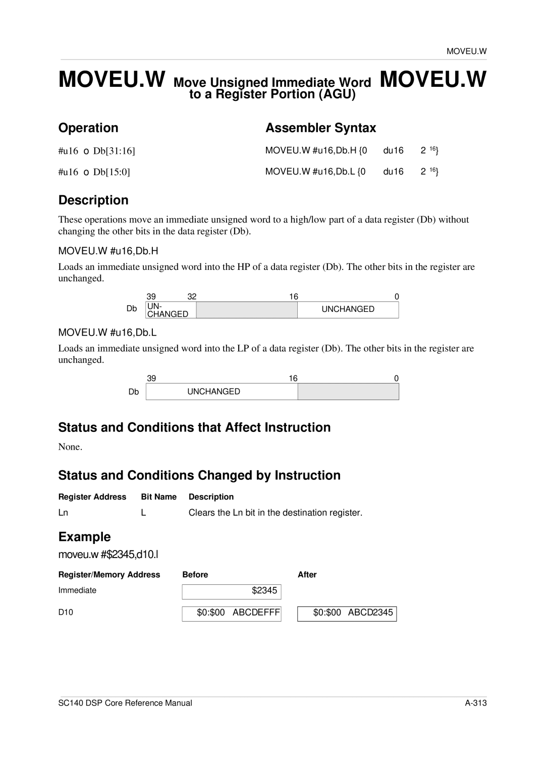
MOVEU.W #u16,Db.H
Moveu.w #$2345,d10.l
#u16 → Db3116
#u16 → Db150
Iiiiiiiiiiiiiiii Bit unsigned immediate data
#u16
MOVEU.W
Move Unsigned Word from
Memory to a Register AGU Operation
Moveu.w r7+2,d10
MOVEU.W a16,C4
318
MPY Da,Db,Dn
MPY
Mpy d4,d5,d6
Da.H * Db.H → Dn
Mpy d6,d6,d7
SC140 DSP Core Reference Manual 321
Mpyr Da,Db,Dn
Mpyr
Mpyr d4,d5,d6
RndDa.H * Db.H → Dn
Register/Memory Address Before After L6D6
$0000
324
Mpysu Dc,Dd,Dn
Mpysu
Mpysu d4,d5,d6
Dc.H * Dd.L → Dn
326
Mpyus
Dc.L * Dd.H → Dn
Mpyus Dc,Dd,Dn
328
Mpyuu Dc,Dd,Dn
Mpyuu
Mpyuu d4,d5,d6
Dc.L * Dd.L → Dn
330
NEG Dn
NEG
Negate Dalu
Neg d3
NEG Dn
Nop
NOP
No Operation Prefix
No operation
~Da → Dn
Not
Bitwise Complement Dalu
Not d4,d5
SC140 DSP Core Reference Manual 335
Binary Inversion of a 16-Bit Operand BMU
Not D0.L
~DR.L → DR.L
Not DR.L
NOT.W
Binary Inversion of a 16-Bit Operand
Memory BMU Operation Assembler Syntax
Not.w r1
Or Da,Dn
Bitwise Inclusive or Dalu
Example or d3,d0
Da Dn → Dn
SC140 DSP Core Reference Manual 341
Or #u16,DR.L
Or #$0f0a,d0.l
#u16 DR.L → DR.L
#u16 DR.H → DR.H
Or #u16,DR.L Or #u16,DR.H
OR.W #u16,a16
OR.W #u16,Rn
OR.W #u16,SP-u5
OR.W #u16,SP+s16
OR.W #u16,Rn
Or.w #$f01a,r1
346
POP Do
SP 8 → De SP 8 → SP
SP 4 → Do SP 8 → SP
POP De
Pop d3
Extension Pairs, Even Registers, and Loop Start Registers
Eeeee
NSP 4 → Do NSP 8 → ΝSP
NSP 8 → De NSP 8 → ΝSP
Popn d6.ed7.e
Popn De
Popn Do
352
Push Do
De → SP SP + 8 → SP
Do → SP + 4 SP + 8 → SP
Push De
Push d0.ed1.e
SC140 DSP Core Reference Manual 355
Pushn Do
De → NSP NSP + 8 → ΝSP
Do → NSP + 4 NSP + 8 → ΝSP
Pushn De
Pushn d0.ed1.e
Pushn De Pushn Do
RND Da,Dn
RND
Round Dalu
RndDa → Dn
Rnd d2,d1
Rnd d1,d5
RND Da,Dn
ROL Dn
Rol d5
Dn3801 → Dn391
Dn39 → C → Dn0
ROL Dn
ROR Dn
Ror d15
Dn39-11 → Dn38-0
→ Dn39 Dn0 → C
ROR Dn
RTE
SP 8 → PC
SP 4 → SR SP 8 → SP → Nmid
Instruction Words Cycles1 Type
Rte
Rted
Trap
Example rted
If RAS valid, then RAS → PC
RTS
Return From Subroutine AGU
Rts
RTS
Rtsd
Rtsd
Rtsd
Register Address Bit Name Description EMR3
Restore PC from Stack AGU
Rtstk
Cleared
Example rtstk
Rtstkd
SP 8 → PC
SP 8 → SP
Example rtstkd
SAT.F Da,Dn
SAT.F
Sat.f d2,d3
If Da $007FFFFFFF then $007FFF0000 → Dn
SAT.F Da,Dn
SAT.L
Sat.l d6
SAT.L Dn
SC140 DSP Core Reference Manual 381
SBC Dc,Dd
SBC
Subtract With Borrow Dalu
Db Dc C → Dd
SBC Dc,Dd
RndDn Da → Dn
SBR
Subtract And Round Dalu
Sbr d3,d0
0010 1010 1110 0111 0000 0000 1000$2AE7
Skipls label
If LCn ≤ Then PC + displacement → PC Skipls label → LFn
Skipls
Skipls label
Skipls label
Stop
Stop Stop Instruction Processing AGU Operation
Enter the stop processing state
SUB #u5,Dn
SUB
Subtract Dalu
Sub d1,d0,d2
Sub d0,d1,d2
SC140 DSP Core Reference Manual 391
SUB2
Subtract Two 16-Bit Values Dalu
Sub2 d0,d1
SUB2 Da,Dn
Suba #u5,Rx
Suba
Subtract AGU
Suba r1,r0
Suba
Dn Da → Dn
Subl
Shift Left and Subtract Dalu
Subl d0,d1
$0$FF Ffff Fffe
SUBNC.W #s16,Dn
SUBNC.W
Subnc.w #$15,d0
Dn #s16 → Dn
SUBNC.W #s16,Dn
Sign-Extension Dalu
Sxt.b d3,d0
Sxt.w d3,d2
Sxt.l d3
Sign-Extension AGU
Sxta.b r3,r1
Sxta.w r3
SXTA.B
Tfr d7,d6
TFR
Transfer Data Register to Data Register Dalu
Tfr d15,d14
TFR Da,Dn
Tfra rx,Rx
Tfra
Tfra r0,r1
Rx → Rx
SC140 DSP Core Reference Manual 407
Else Rn → ESP
To/from a Register AGU
If Srexp = Then NSP → Rn
Else ESP → Rn If Srexp = Then Rn → NSP
Tfra r0,osp
Tfrt Da, Dn
Tfrt d14,d15
If T=1, then Da → Dn
If T=0, then Da → Dn
Tfrt
TRAPn
Trap Execute a Software Exception AGU Trap Operation
Trap
If Dn == 0, then 1 → T, else 0 → T
Tsteq
Test for Equal to Zero Dalu
Tsteq d1
TSTEQA.W Rx
TSTEQA.x Test for Equal to Zero AGU TSTEQA.x Operation
Tsteqa.w r4
Tsteqa.l r1
TSTEQA.W TSTEQA.L
If Dn = 0, then 1 → T, else 0 → T
Tstge
Test for Greater Than Or Equal to Zero Dalu
Tstge d4
Tstgea.l r7
If Rx ≥ 0, then 1 → T, else 0 → T
TESTGEA.L Rx
TSTGEA.L Rx
Tstgt Dn
Tstgt Test for Greater Than Zero Dalu Tstgt Operation
Tstgt d6
If Dn 0, then 1 → T, else 0 → Τ
Tstgta Rx
Tstgta Test for Greater Than Zero AGU Tstgta Operation
Tstgta r2
If Rx 0, then 1 → T, else 0 → Τ
Viterbi Shift Left Move AGU
Word Big Endian Mode
Little Endian Mode
VSL
VSL.2F D1D3,Rn+N0
VSL.4W D2D6D1D3,Rn+N0
VSL.4F D2D6D1D3,Rn+N0
VSL.2W D1D3,Rn+N0
Vsl.2w d1d3,r0+n0
After Little Endian
After Big Endian
VSL.4W
Response
Enters the low-power standby Wait processing
Wait
State
Wait
Zero Extension Dalu
Zxt.b d2,d5
Zxt.w d3,d6
Zxt.l d0
Zero Extension AGU
Zxta.b r3,n2
Zxta.w r4
ZXTA.B
ZXTA.x 432
Appendix B StarCore Registry
Using the StarCore Registry
Table B-1. Scid Assignments
Hex Bits Instruction Cores Example
Set Version SoC / platform
Index
Ecnten
Eeddef
Eselctrl 4-26ESELDI 4-26ESELDM 4-26ESELDTB 4-26 Eseletb
MOVES.F A-299 MOVES.L A-301 MOVEU.B A-307
Macsu A-239 Macus A-241 Macuu A-243
Mpysu A-325 Mpyus A-327 Mpyuu A-329
Rtstk A-374
Index
Index
SC140 DSP Core Reference Manual