www.ti.com
SRIO Registers
5.34 LSUn Control Register 1 (LSUn_REG1)
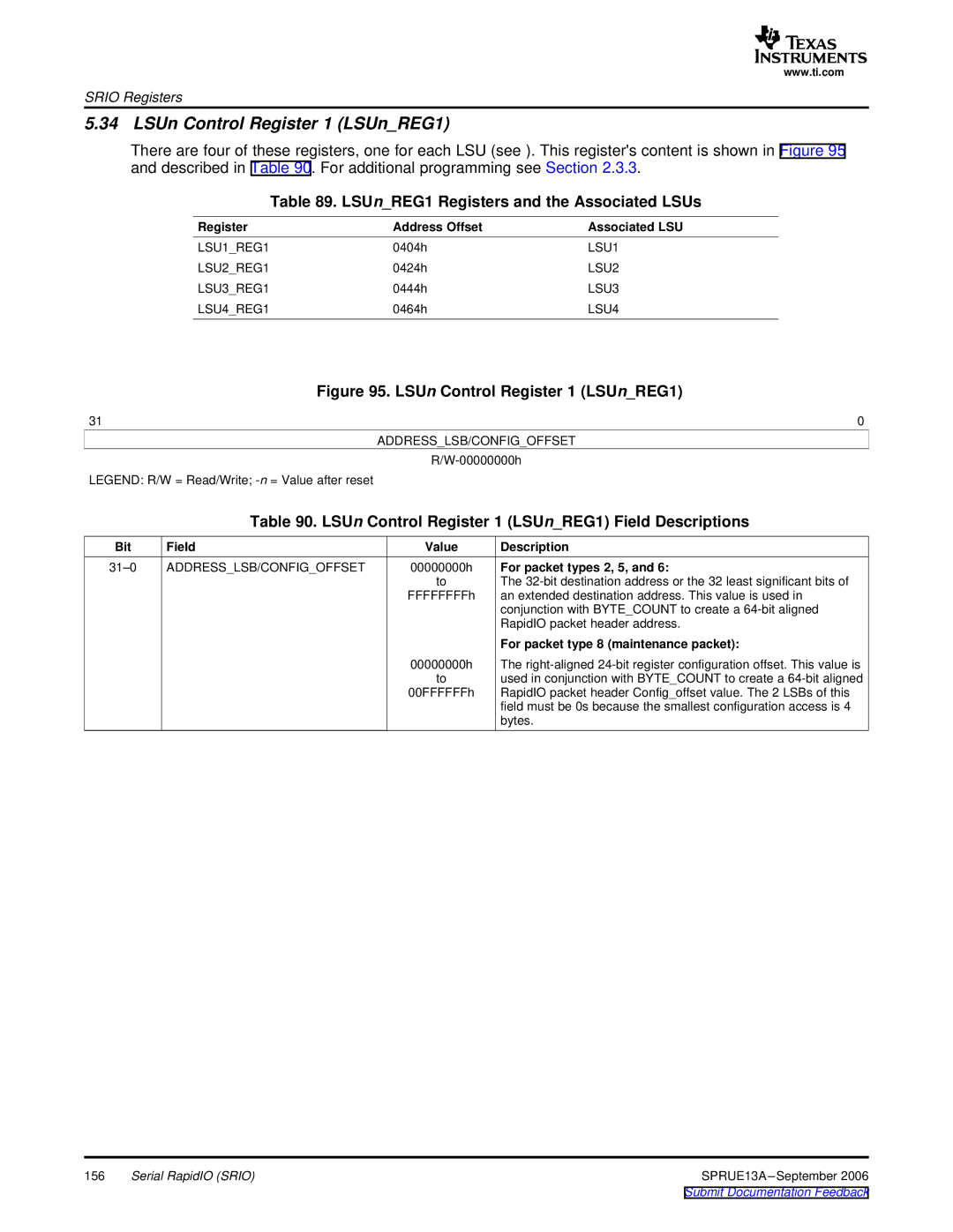
There are four of these registers, one for each LSU (see ). This register'scontent is shown in Figure 95 and described in Table 90. For additional programming see Section 2.3.3.
Table 89. LSUn_REG1 Registers and the Associated LSUs
Register | Address Offset | Associated LSU |
LSU1_REG1 | 0404h | LSU1 |
LSU2_REG1 | 0424h | LSU2 |
LSU3_REG1 | 0444h | LSU3 |
LSU4_REG1 | 0464h | LSU4 |
| Figure 95. LSUn Control Register 1 (LSUn_REG1) |
31 | 0 |
ADDRESS_LSB/CONFIG_OFFSET
LEGEND: R/W = Read/Write;
Table 90. LSUn Control Register 1 (LSUn_REG1) Field Descriptions
Bit | Field | Value | Description |
ADDRESS_LSB/CONFIG_OFFSET | 00000000h | For packet types 2, 5, and 6: | |
|
| to | The |
|
| FFFFFFFFh | an extended destination address. This value is used in |
|
|
| conjunction with BYTE_COUNT to create a |
|
|
| RapidIO packet header address. |
|
|
| For packet type 8 (maintenance packet): |
|
| 00000000h | The |
|
| to | used in conjunction with BYTE_COUNT to create a |
|
| 00FFFFFFh | RapidIO packet header Config_offset value. The 2 LSBs of this |
|
|
| field must be 0s because the smallest configuration access is 4 |
|
|
| bytes. |
156 | Serial RapidIO (SRIO) | SPRUE13A |
