www.ti.com

SRIO Functional Description

2.3.2SERDES Macro and its Configurations

SRIO offers many benefits to customers by allowing a scalable non-proprietary interface. With the use of TI’s SERDES macros, the peripheral is very adaptable and bandwidth scalable. The same peripheral can be used for all three frequency nodes specified in V1.2 of the RapidIO Interconnect Specification (1.25, 2.5, and 3.125 Gbps). This allows you to design to only one protocol throughout the system and selectively choose the bandwidth, thus eliminating the need for user’s proprietary protocols in many instances, and providing a faster design turn and production ramp. Since this interface is serial, the application space is not limited to a single board. It will propagate into backplane applications as well. Integration of these macros on an ASIC or DSP allows you to reduce the number of discrete components on the board and eliminates the need for bus driver chips.

Additionally, there are some valuable features built into TI SERDES. System optimization can be uniquely managed to meet individual customer applications. For example, control registers within the SERDES allow you to adjust the TX differential output voltage (Vod) on a per driver basis. This allows power savings on short trace links (on the same board) by reducing the TX swing. Similarly, data edge rates can be adjusted through the control registers to help reduce any EMI affects. Unused links can be individually powered down without affecting the working links.

The SERDES macro is a self-contained macro which includes transmitter (TX), receiver (RX), phase-locked-loop (PLL), clock recovery, serial-to-parallel (S2P), and parallel-to-serial (P2S) blocks. The internal PLL multiplies a user-supplied reference clock. All loop filter components of the PLL are onchip. Likewise, the differential TX and RX buffers contain on-chip termination resistors. The only off-chip component requirement is for DC blocking capacitors.

2.3.2.1Enabling the PLL

The Physical layer SERDES has a built-in PLL, which is used for the clock recovery circuitry. The PLL is responsible for clock multiplication of a slow speed reference clock. This reference clock has no timing relationship to the serial data and is asynchronous to any CPU system clock. The multiplied high-speed clock is only routed within the SERDES block; it is not distributed to the remaining blocks of the peripheral, nor is it a boundary signal to the core of the device. It is extremely important to have a good quality reference clock, and to isolate it and the PLL from all noise sources. Since RapidIO requires 8-bit/10-bit encoded data, the 8-bit mode of the SERDES PLL is not be used.

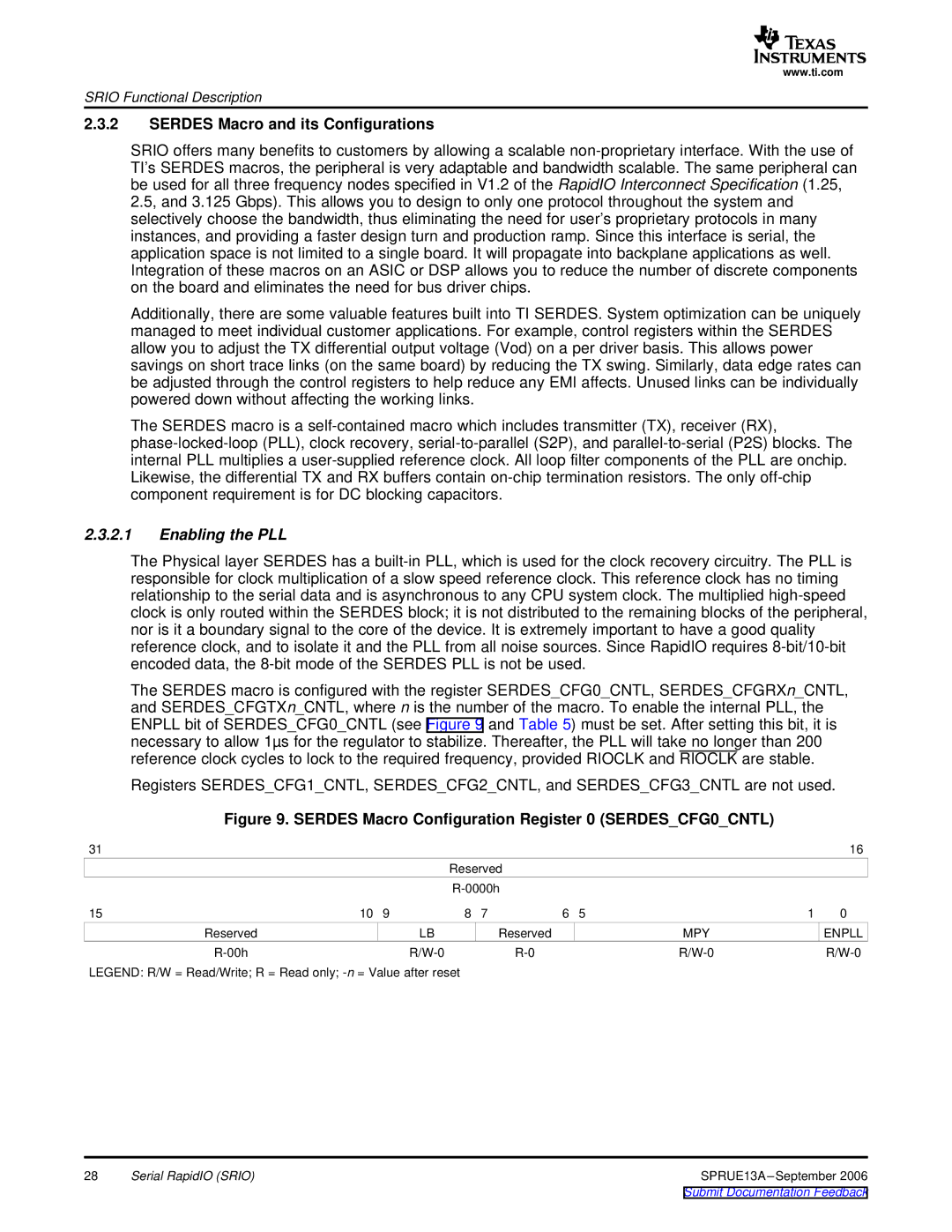
The SERDES macro is configured with the register SERDES_CFG0_CNTL, SERDES_CFGRXn_CNTL, and SERDES_CFGTXn_CNTL, where n is the number of the macro. To enable the internal PLL, the ENPLL bit of SERDES_CFG0_CNTL (see Figure 9 and Table 5) must be set. After setting this bit, it is necessary to allow 1µs for the regulator to stabilize. Thereafter, the PLL will take no longer than 200 reference clock cycles to lock to the required frequency, provided RIOCLK and RIOCLK are stable.

Registers SERDES_CFG1_CNTL, SERDES_CFG2_CNTL, and SERDES_CFG3_CNTL are not used.

Figure 9. SERDES Macro Configuration Register 0 (SERDES_CFG0_CNTL)

31


16


Reserved


R-0000h


15

10

9

8

7

6

5

1

0

Reserved


LB


Reserved


MPY

ENPLL

R-00h


R/W-0


R-0


R/W-0

R/W-0

LEGEND: R/W = Read/Write; R = Read only; -n= Value after reset

28

Serial RapidIO (SRIO)

SPRUE13A –September 2006


Submit Documentation Feedback

Page 28
Image 28
Texas Instruments TMS320TCI648x manual Serdes Macro and its Configurations, Enabling the PLL, MPY Enpll