www.ti.com
SRIO Registers
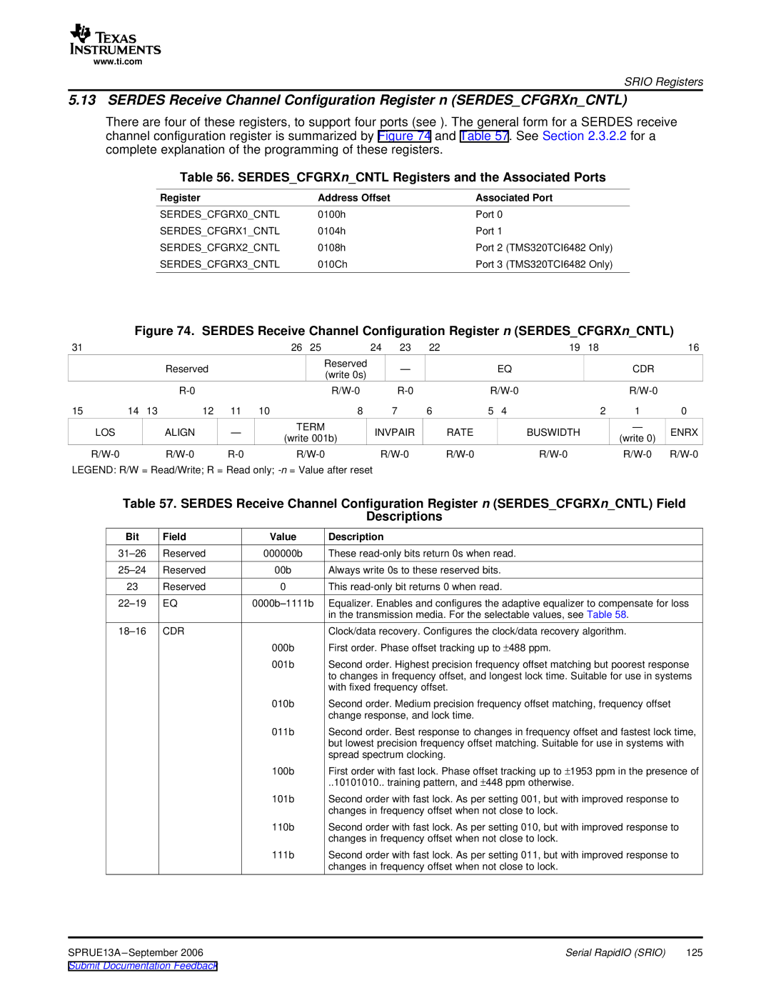
5.13 SERDES Receive Channel Configuration Register n (SERDES_CFGRXn_CNTL)
There are four of these registers, to support four ports (see ). The general form for a SERDES receive channel configuration register is summarized by Figure 74 and Table 57. See Section 2.3.2.2 for a complete explanation of the programming of these registers.
Table 56. SERDES_CFGRXn_CNTL Registers and the Associated Ports
Register | Address Offset | Associated Port |
SERDES_CFGRX0_CNTL | 0100h | Port 0 |
SERDES_CFGRX1_CNTL | 0104h | Port 1 |
SERDES_CFGRX2_CNTL | 0108h | Port 2 (TMS320TCI6482 Only) |
SERDES_CFGRX3_CNTL | 010Ch | Port 3 (TMS320TCI6482 Only) |
Figure 74. SERDES Receive Channel Configuration Register n (SERDES_CFGRXn_CNTL)
31 |
|
|
|
|
| 26 | 25 | 24 | 23 | 22 |
|
| 19 | 18 |
| 16 |
|
|
| Reserved |
|
|
| Reserved |
| — |
|
| EQ |
|
| CDR |
|
|
|
|
|
|
| (write 0s) |
|
|
|
|
|
| ||||
|
|
|
|
|
|
|
|
|
|
|
|
|
|
|
| |
|
|
|
|
|
|
|
|
|
|
| ||||||
15 | 14 | 13 | 12 | 11 | 10 |
| 8 |
| 7 | 6 | 5 | 4 |
| 2 | 1 | 0 |
LOS |
|
| ALIGN | — |
| TERM | INVPAIR |
| RATE |
| BUSWIDTH |
| — | ENRX | ||
|
|
| (write 001b) |
|
|
| (write 0) | |||||||||
|
|
|
|
|
|
|
|
|
|
|
|
|
| |||
|
|
|
|
|
| |||||||||||
LEGEND: R/W = Read/Write; R = Read only; |
|
|
|
|
|
|
|
| ||||||||
Table 57. SERDES Receive Channel Configuration Register n (SERDES_CFGRXn_CNTL) Field
Descriptions
Bit | Field | Value | Description |
Reserved | 000000b | These | |
Reserved | 00b | Always write 0s to these reserved bits. | |
23 | Reserved | 0 | This |
EQ | Equalizer. Enables and configures the adaptive equalizer to compensate for loss | ||
|
|
| in the transmission media. For the selectable values, see Table 58. |
CDR |
| Clock/data recovery. Configures the clock/data recovery algorithm. | |
|
| 000b | First order. Phase offset tracking up to ±488 ppm. |
|
| 001b | Second order. Highest precision frequency offset matching but poorest response |
|
|
| to changes in frequency offset, and longest lock time. Suitable for use in systems |
|
|
| with fixed frequency offset. |
|
| 010b | Second order. Medium precision frequency offset matching, frequency offset |
|
|
| change response, and lock time. |
|
| 011b | Second order. Best response to changes in frequency offset and fastest lock time, |
|
|
| but lowest precision frequency offset matching. Suitable for use in systems with |
|
|
| spread spectrum clocking. |
|
| 100b | First order with fast lock. Phase offset tracking up to ±1953 ppm in the presence of |
|
|
| ..10101010.. training pattern, and ±448 ppm otherwise. |
|
| 101b | Second order with fast lock. As per setting 001, but with improved response to |
|
|
| changes in frequency offset when not close to lock. |
|
| 110b | Second order with fast lock. As per setting 010, but with improved response to |
|
|
| changes in frequency offset when not close to lock. |
|
| 111b | Second order with fast lock. As per setting 011, but with improved response to |
|
|
| changes in frequency offset when not close to lock. |
SPRUE13A | Serial RapidIO (SRIO) | 125 |
Submit Documentation Feedback |
|
|