www.ti.com
SRIO Registers
5.36 LSUn Control Register 3 (LSUn_REG3)
There are four of these registers, one for each LSU (see Table 93). LSUn_REG3 is shown in Figure 97 and described in Table 94. For additional programming see Section 2.3.3.
Table 93. LSUn_REG3 Registers and the Associated LSUs
Register | Address Offset | Associated LSU |
LSU1_REG3 | 040Ch | LSU1 |
LSU2_REG3 | 042Ch | LSU2 |
LSU3_REG3 | 044Ch | LSU3 |
LSU4_REG3 | 046Ch | LSU4 |
|
|
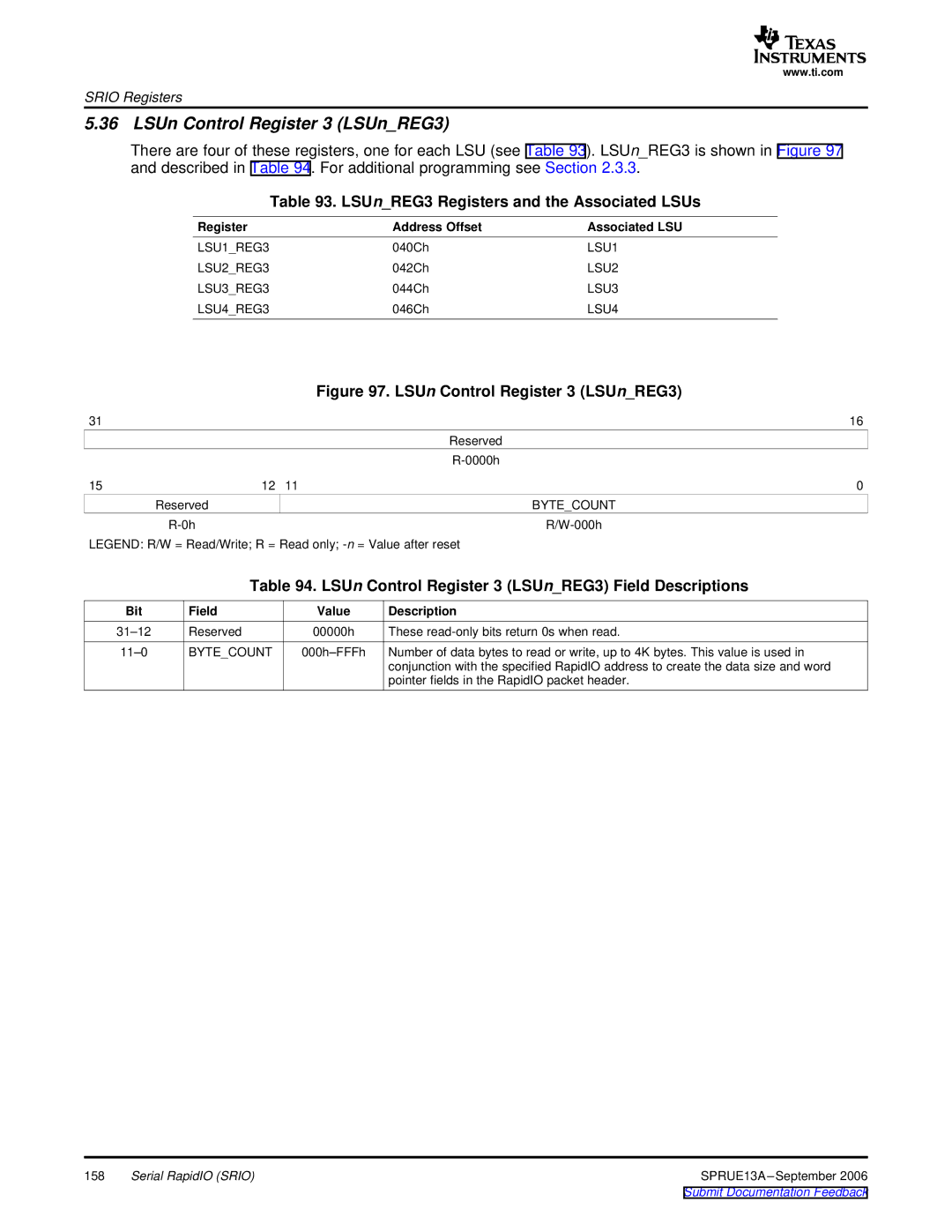
| Figure 97. LSUn Control Register 3 (LSUn_REG3) |
31 |
|
| 16 |
|
|
| Reserved |
|
|
| |
15 | 12 | 11 | 0 |
| Reserved |
| BYTE_COUNT |
|
|
LEGEND: R/W = Read/Write; R = Read only;
Table 94. LSUn Control Register 3 (LSUn_REG3) Field Descriptions
Bit | Field | Value | Description |
Reserved | 00000h | These | |
BYTE_COUNT | Number of data bytes to read or write, up to 4K bytes. This value is used in | ||
|
|
| conjunction with the specified RapidIO address to create the data size and word |
|
|
| pointer fields in the RapidIO packet header. |
158 | Serial RapidIO (SRIO) | SPRUE13A |