www.ti.com
SRIO Registers
5.7Block n Enable Register (BLKn_EN)
There are nine of these registers, one for each of nine logical blocks in the peripheral. The registers and the blocks they support are listed in Table 46. The general form for a block n enable register (BLKn_EN) is shown in Figure 68 and described in Table 47. For additional programming information, see
Section 2.3.10.
Table 46. Block n Enable Registers and the Associated Blocks
Register | Address Offset | Associated Block |
BLK0_EN | 0038h | Logical block 0: the set of |
|
| peripheral |
BLK1_EN | 0040h | Logical block 1: the Load/Store module (the four LSUs and supporting logic) |
BLK2_EN | 0048h | Logical block 2: the memory access unit (MAU) |
BLK3_EN | 0050h | Logical block 3: the message transmit unit (TXU) |
BLK4_EN | 0058h | Logical block 4: the message receive unit (RXU). |
BLK5_EN | 0060h | Logical block 5: SRIO port 0 |
BLK6_EN | 0068h | Logical block 6: SRIO port 1. |
BLK7_EN | 0070h | Logical block 7: SRIO port 2. |
BLK8_EN | 0078h | Logical block 8: SRIO port 3. |
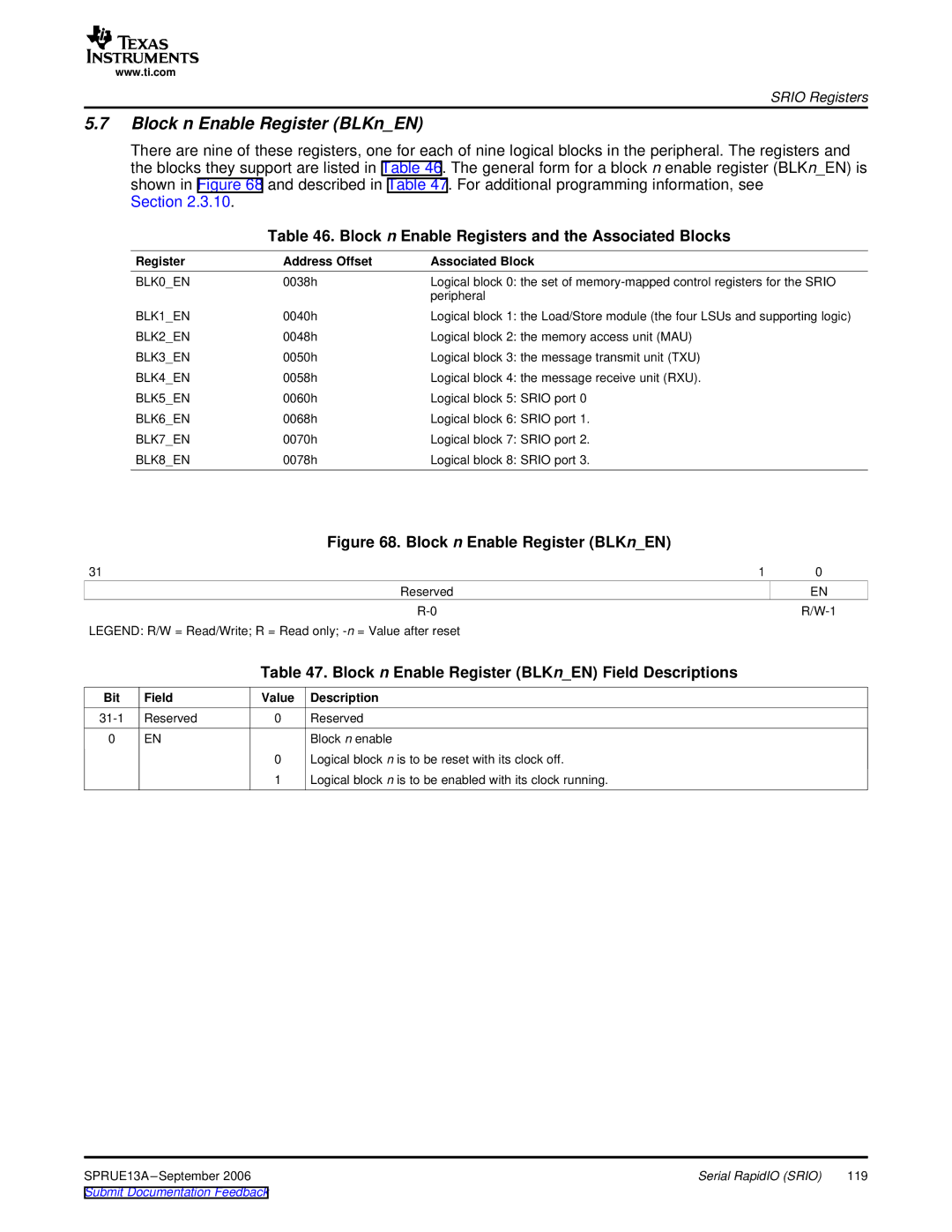
Figure 68. Block n Enable Register (BLKn_EN)
31 | 1 | 0 |
Reserved |
| EN |
| ||
LEGEND: R/W = Read/Write; R = Read only; |
|
|
Table 47. Block n Enable Register (BLKn_EN) Field Descriptions
Bit | Field | Value | Description |
Reserved | 0 | Reserved | |
0 | EN |
| Block n enable |
|
| 0 | Logical block n is to be reset with its clock off. |
|
| 1 | Logical block n is to be enabled with its clock running. |
SPRUE13A | Serial RapidIO (SRIO) | 119 |
Submit Documentation Feedback |
|
|