www.ti.com
SRIO Registers
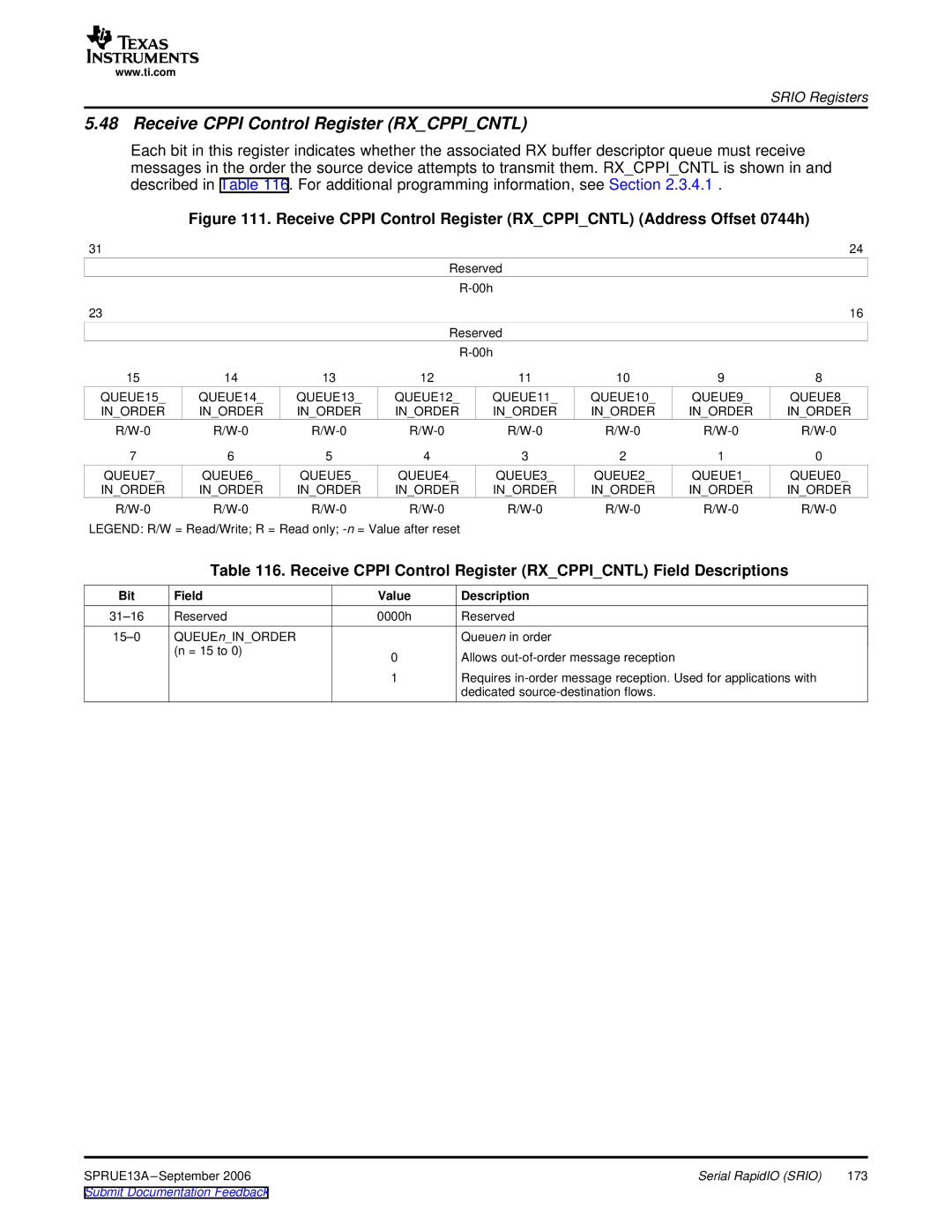
5.48 Receive CPPI Control Register (RX_CPPI_CNTL)
Each bit in this register indicates whether the associated RX buffer descriptor queue must receive messages in the order the source device attempts to transmit them. RX_CPPI_CNTL is shown in and described in Table 116. For additional programming information, see Section 2.3.4.1 .
Figure 111. Receive CPPI Control Register (RX_CPPI_CNTL) (Address Offset 0744h)
31 |
|
|
|
|
|
| 24 |
|
|
| Reserved |
|
|
| |
|
|
|
|
|
| ||
23 |
|
|
|
|
|
| 16 |
|
|
| Reserved |
|
|
| |
|
|
|
|
|
| ||
15 | 14 | 13 | 12 | 11 | 10 | 9 | 8 |
QUEUE15_ | QUEUE14_ | QUEUE13_ | QUEUE12_ | QUEUE11_ | QUEUE10_ | QUEUE9_ | QUEUE8_ |
IN_ORDER | IN_ORDER | IN_ORDER | IN_ORDER | IN_ORDER | IN_ORDER | IN_ORDER | IN_ORDER |
7 | 6 | 5 | 4 | 3 | 2 | 1 | 0 |
QUEUE7_ | QUEUE6_ | QUEUE5_ | QUEUE4_ | QUEUE3_ | QUEUE2_ | QUEUE1_ | QUEUE0_ |
IN_ORDER | IN_ORDER | IN_ORDER | IN_ORDER | IN_ORDER | IN_ORDER | IN_ORDER | IN_ORDER |
LEGEND: R/W = Read/Write; R = Read only;
Table 116. Receive CPPI Control Register (RX_CPPI_CNTL) Field Descriptions
Bit | Field | Value | Description |
Reserved | 0000h | Reserved | |
QUEUEn_IN_ORDER |
| Queuen in order | |
| (n = 15 to 0) | 0 | Allows |
|
| ||
|
| 1 | Requires |
|
|
| dedicated |
SPRUE13A | Serial RapidIO (SRIO) | 173 |