www.ti.com
SRIO Registers
5.33 LSUn Control Register 0 (LSUn_REG0)
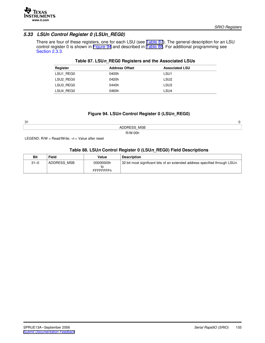
There are four of these registers, one for each LSU (see Table 87). The general description for an LSU control register 0 is shown in Figure 94 and described in Table 88. For additional programming see Section 2.3.3.
Table 87. LSUn_REG0 Registers and the Associated LSUs
Register | Address Offset | Associated LSU |
LSU1_REG0 | 0400h | LSU1 |
LSU2_REG0 | 0420h | LSU2 |
LSU3_REG0 | 0440h | LSU3 |
LSU4_REG0 | 0460h | LSU4 |
| Figure 94. LSUn Control Register 0 (LSUn_REG0) |
31 | 0 |
ADDRESS_MSB
LEGEND: R/W = Read/Write;
Table 88. LSUn Control Register 0 (LSUn_REG0) Field Descriptions
Bit | Field | Value | Description |
ADDRESS_MSB | 00000000h | ||
|
| to |
|
|
| FFFFFFFFh |
|
SPRUE13A | Serial RapidIO (SRIO) | 155 |
Submit Documentation Feedback |
|
|