Fault Screen Display | Possible Causes |
|
|
|
|
Typeform Error | • Firmware information (typeform) loaded into the Gate Driver board is |
| inconsistent with the device in which the firmware is being used. |
| • The Gate Driver board has been replaced. |
| • The Gate Driver board is defective. |
|
|
U Phase Short Circuit | • Low impedance at the U lead of the ASD output. |
|
|
V Phase Short Circuit | • Low impedance at the V lead of the ASD output. |
|
|
W Phase Short Circuit | • Low impedance at the W lead of the ASD output. |
|
|
Note: The event that caused the Trip(s) must be corrected or must decrease to less than the threshold value required to cause the trip to allow for a Reset to be recognized. In the event of multiple active trips, the trip displayed will remain until all faults are corrected and all trips are cleared.
Viewing Trip Information
In the event that the condition causing an Alarm does not return to the normal operating level within a specified time, the ASD Faults and a Trip is incurred.
When a trip occurs, the resultant error information may be viewed either from the Trip History screen (Program ⇒ Monitor Setup ⇒ Trip History), the Trip Monitor From ASD screen (Program ⇒ Monitor Setup ⇒ Trip Monitor From ASD), or from the Monitor screen.
Trip History
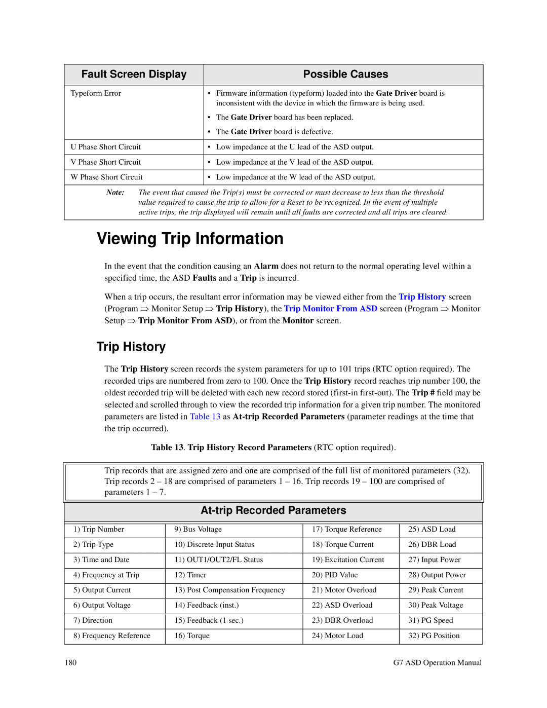
The Trip History screen records the system parameters for up to 101 trips (RTC option required). The recorded trips are numbered from zero to 100. Once the Trip History record reaches trip number 100, the oldest recorded trip will be deleted with each new record stored
Table 13. Trip History Record Parameters (RTC option required).
Trip records that are assigned zero and one are comprised of the full list of monitored parameters (32). Trip records 2 – 18 are comprised of parameters 1 – 16. Trip records 19 – 100 are comprised of parameters 1 – 7.
At-trip Recorded Parameters
1) | Trip Number | 9) Bus Voltage | 17) | Torque Reference | 25) | ASD Load | |
|
|
|
|
|
|
|
|
2) | Trip Type | 10) | Discrete Input Status | 18) | Torque Current | 26) | DBR Load |
|
|
|
|
|
|
| |
3) | Time and Date | 11) OUT1/OUT2/FL Status | 19) | Excitation Current | 27) | Input Power | |
|
|
|
|
|
|
|
|
4) | Frequency at Trip | 12) | Timer | 20) | PID Value | 28) | Output Power |
|
|
|
|
|
|
|
|
5) | Output Current | 13) | Post Compensation Frequency | 21) | Motor Overload | 29) | Peak Current |
|
|
|
|
|
|
|
|
6) | Output Voltage | 14) | Feedback (inst.) | 22) | ASD Overload | 30) | Peak Voltage |
|
|
|
|
|
|
|
|
7) | Direction | 15) | Feedback (1 sec.) | 23) | DBR Overload | 31) | PG Speed |
|
|
|
|
|
|
|
|
8) | Frequency Reference | 16) | Torque | 24) | Motor Load | 32) | PG Position |
|
|
|
|
|
|
|
|
180 | G7 ASD Operation Manual |
