G7 ASD Control
The Control PCB (P/N 56000) serves as the primary control source for the G7 ASD and receives input from the Control Terminal Strip PCB (see Figure 6 on pg. 25), an Option Card, RS232/RS485 Communications, or the EOI.
The Control PCB has been enhanced to support two new functions: Multiple Protocol Communications and the ability to communicate in either half- or
Using the optional
NANOCOM.
The
Half or Full duplex communications is available when using RS232/RS485 communications. The jumpers at the JP1 and the JP2 connectors may be moved from one position to the other to facilitate either half- or
For more information on the G7 ASD communication requirements, please visit WWW.TIC.TOSHIBA.COM to acquire a copy of the
Contact your Toshiba representative if more information is required on the
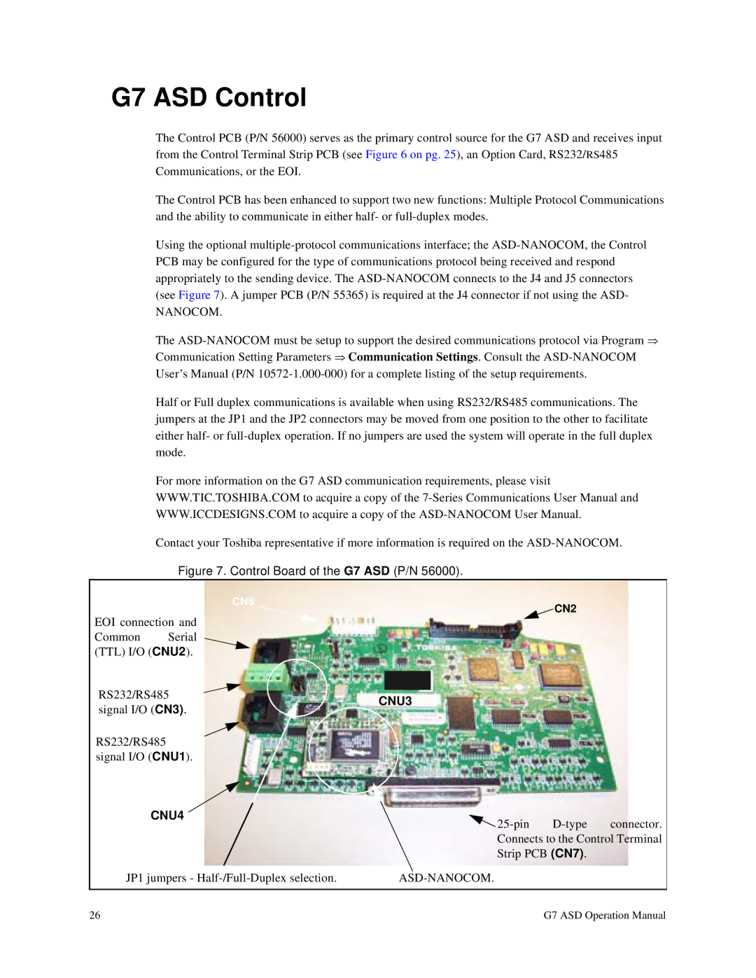
Figure 7. Control Board of the G7 ASD (P/N 56000).
CN8
EOI connection and
Common Serial (TTL) I/O (CNU2).
 CN2
CN2
RS232/RS485 |
|
| |
CNU3 | |||
signal I/O (CN3). | |||
|
| ||
RS232/RS485 signal I/O (CNU1).
CNU4 | |
| |
| Connects to the Control Terminal |
| Strip PCB (CN7). |
JP1 jumpers - |
26 | G7 ASD Operation Manual |