Page
FLD=, FAND=, FAND, FAND, Fand
DVP-ES2/EX2/SS2/SA2/SX2/SE
Page
Contents
Communications
Appendix a
Series Model name
Page
PLC Concepts
PLC Scan Method
Reverse Current
Current Flow
No Contact, NC Contact
Scan time exception
PLC Registers and Relays
Ladder Logic Symbols
Creating a PLC Ladder Program
2 LD / LDI Load no contact / Load NC contact
ORB ANB
TMR
MPS / MRD / MPP Branch instructions
ANB Connect block in series
ORB Connect block in parallel
STL Step Ladder Programming
Branch Description Instruction Symbol
MPS
RET Return
S21 S22
Ladder Diagram
Conversion between Ladder Diagram and Instruction List Mode
Example Good method Bad method
Common Programming Errors
Fuzzy Syntax
Example Better method OK method
Or operation upward is not allowed Reverse current exists
Or T0
Correcting Ladder Diagram
Example
LD T0 X2 ORB
OUT Y0 Y1 and X0 OUT Y1
MPS OUT MPP
Example 1 Stop First latched circuit
Basic Program Design Examples
Example 3 Latched circuit of SET and RST
Example 4 Power down latched circuit
Example 2 Start First latched circuit
Stop
Example 8 Oscillating Circuit
Example 6- Interlock control
Example 7 Sequential Control
Example 11 Trigger Circuit
Example 9 Oscillating Circuit with Timer
Example 12 Delay OFF Circuit
Example 10 Flashing Circuit
Example 15 Counting Range Extension Circuit
Example 13 Output delay circuit
Example 14 Timing extension circuit
SFC Figure
Timing Diagram
Green light
Green light Blinking
Ladder Diagram
WPLSoft programming SFC mode
Memo
Programming Concepts
ES2/EX2 Memory Map
Specifications
Programming Concepts
Specifications
SS2 Memory Map
Specifications
Specifications
SA2 Memory Map
Specifications
Specifications
SX2 Memory Map
Specifications
Specifications
OFF=ON
Status and Allocation of Latched Memory
STOP=RUN RUN=STOP
Binary, Octal, Decimal, BCD, Hex
PLC Bits, Nibbles, Bytes, Words, etc
HEX
BCD
BIN OCT DEC
EX2 RUN Stop
Relay
Latch Default Function
M1052 Disable interruption I200
OFF PCC01
M1109 Y1 pulse output pause ramp down
M1141 For COM2 RS-485, Modrd / Modwr
M1203 C203 counting mode on count down
M1233 C233 counter monitor on count down
M1274 C239 counting mode on falling-edge
OFF YES
M1378 Indicate Slave ID#3 data interchange
Latch Default
Attrib Latch Default
Timer
Bits Bits counters Counters
Accumulative Timer
Timers for Subroutines and Interrupts
Counter
RST CNT OUT
Plus 1 or count down minus
OUT Y0
Applicable Software High Speed Counters
High-speed Counters
Applicable Hardware High Speed Counters
Dcnt
Phase 1 input high-speed counter Example
RST
Phase 2 inputs high-speed counter Example
MOV
AB-phase input high-speed counter Example
0FDB
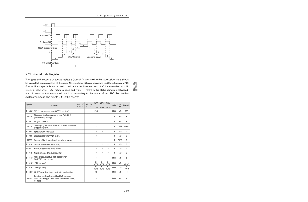
Special Data Register
D1031 PV of Y0 pulse output High word
YES ’FFFF
COM2RS-485 Definition of start character STX ’3A
D1240 stores the low word of high-speed counter
D1314 Minute of RTC 00 ~
’1064
Link
D1442 Data length to be read on Slave ID#9
PLC Link
D1767 D1768 Data which is read from slave ID#10
DVP-PCC01
Call
14 E, F Index Registers
Nest Level PointerN, PointerP, Interrupt Pointer
Index register E, F
CJ P1
Call
Page
Applications of Special M Relays and D Registers
Function Group Watchdog Timer Number M1008, D1008 Contents
Number D1002 Contents
Function Group High-speed Timer Number M1015, D1015 Contents
Device Name Function
Function Group Number D1018~D1019 Contents
Number M1083,M1084, D1023 Contents
Number D1020 Contents
RAMP, Sort
MTR, HKY, DSW, SEGL, PR
PLSY, Plsr
Incd
Device Devices will be cleared
Number M1034 Contents
Dabsr
ZRN, DRVI, Drva
COM1 COM2 COM3
Function Group RUN/STOP Switch Number M1035 Contents
Content
Port
Example 2 Modiying COM2 communication format
COM3
Example 1 Modifying COM1 communication format
Example 3 Modifying COM3 communication format
Example 4 RTU mode setting of COM1、COM2、COM3
Number D1038 Contents
Number M1037, D1037 Contents
Number D1062, D1110~D1113, D1116~D1118 Contents
Function Group Fixed scan time Number M1039, D1039 Contents
Device Function
0xF
Number M1119 Contents
STOP→RUN RUN→STOP
Contents Device Explanation Latched
Error code explanation D1067 error code Function
Number M1280, M1284, M1286 Contents
Number M1308, D1312 Contents
Number M1304 Contents
Function Group PLC Link Number
Number D1320~ D1327 Contents
Number M1346 Contents
Master PLC Slave ID
Read Write Out D100 D200
M1376 M1377 M1378 M1379 M1380 M1381 M1382 M1383
M1416 M1417 M1418 M1419 M1420 M1421 M1422 M1423
Page
Programming Concepts
Operation flow chart
Programming Concepts
SET MOV
Programming Concepts
Memo
Instruction Set
ES2/EX2/SS2 SA2/SX2
Basic Instructions without API numbers
Execution speed Instruction Function Operand Steps
LDI
Explanations to Basic Instructions
ORI
ANI
Connect NC contact Series Controllers
Connect no contact Parallel Controllers
ORB
Mnemonic Function Program steps
ANB
Connect a block in series Controllers
Points to note
Explanations Controllers
OUT
MPS
MRD
MPP
RST
SET
Latches the on Status Controllers
Device Status
MCR
No operation Controllers
END
Program End Controllers
NOP
Scan cycle
Fend
Pointers
Interrupt Pointers
P10
Communication Interrupts
Timer Interrupts
Iret
External interrupt
Type Bit Devices Word devices Program Steps
Application Programming Instructions
API
Mnemonic Operands Function Controllers
Explanation of the format of application instruction
Length of Operand 16-bit or 32-bit instruction
Operand Data format
Continuous execution vs. Pulse execution
Flags Bit instruction
Kn values Bit instruction
API 155 Dabsr
Limitations for times of using instructions
Numeric Values
Limitation of synchronized execution
Floating Point Operation
Assign Continuous Bit Numbers
Decimal Floating Point
Binary Floating Point
Example 1 Represent 23 in 32-bit floating point value
Example 2 Represent -23.0 in 32-bit floating point value
Bit 16-bit 32-bit
Instruction Set
Four Arithmetic Operations
Loop Control
Transmission Comparison
Data Processing
Rotation and Displacement
External I/O Display
High Speed Processing
Handy Instructions
Basic Instructions
Serial I/O
Falling-edge output Communication Instructions
PLF
Additional Instruction
Real Time Calendar
Positioning Control
Contact Type Logic Operation
Gray Code
Matrix Operation
Specific Bit Control
223
DOR
S1 S2 Contact Type Comparison
Absd Dabsd
Numerical List of Instructions in alphabetic order
ABS Dabs
Alternate state 218
Connect NC contact in parallel By specified bit 266
GPS data receiving 144
PLF
Pulse output Print Ascii code output
Stop VFD
Axis Relative Position Arc Interpolation 197
Single-Axis pulse output by 116
Range
Detailed Instruction Explanation
CJ P1
M4 on OFF
OFF→ON
ON→OFF M4 OFF M4 OFF→ON
M4 on
CNT
CALL, Callp 3 steps
Descriptions Program Steps
Mnemonic Function
Sret
Subroutine Return
INC
Interrupt Return
Mnemonic Function Enable Interrupt Controllers
Mnemonic Function Disable Interrupt Controllers
Iret
Flag Function
101
No contact to drive the instruction is required
Fend
End of The Main Program First End
CJ Instruction Program Flow
Call Instruction Program Flow
WDT, Wdtp 1 step
WDT
KnX KnY KnM KnS T For 3 steps
For K3 For K4 Next
TMR
CMP
ZCP
Mnemonic Operands Function
RST M0 RST M1 RST M2 Zrst M0 M2
KnX KnY KnM KnS T MOV, Movp 5 steps
Shift
Smov
PLC
CML
BMOV, Bmovp 7 steps
Bmov K1M0 K1Y0
DFMOV, Dfmovp
Fmov
XCH
BCD
BIN
103 102 101 Digit DIP switch in BCD format
Operation of flags
ADD
Zero flag
16-bit BIN subtraction
SUB
MUL
MUL D0 D10 D20
B00 B15
DIV
INC
DEC
Wand
D2 0
Dand
Logical Word or
WOR
DOR
Logical DWord or
Logical Word XOR
Wxor
Dxor
NEG
D0=2 0 0
ROR
ROL
RCR
RCL
KnX KnY KnM KnS T SFTR, Sftrp 9 steps
Sftr
Word Shift Right
Wsfr
Wsfrp K1X20 K1Y20
Word Shift Left
Wsfl
KnX KnY KnM KnS SFWR, Sfwrp 7 steps
Shift Register Read
Sfrd
KnX KnY KnM KnS T ZRST, Zrstp 5 steps
RST M0 RST T0 RST Y0
KnX KnY KnM KnS DECO, Decop 7 steps
D10 D20 B15 All be
All be B15
D10
SUM
BON
DMEAN, Dmeanp
Mean
ANS T10 K50 S999
Points to note Flags
Application example of alarm device production line
Instruction driven by contact is necessary
ANS
SQR
FLT
Apply FLT instruction to complete the following operation
FLT
KnX KnY KnM KnS T REF, Refp 5 steps
SET M1180
KnX KnY KnM KnS T REFF, Reffp 3 steps
MTR
MTR
Points to note
Hscs
Instruction Set
Page
Counting
Dhscs K100
Fend
Hscr
API Mnemonic Operands Function Controllers
Compare Type Bit Devices Word devices Program Steps
HSZ
High Speed Zone
Page
Dhsz
Program Example 1 Applying Hardware High Speed Counter
Speed variable
KnX KnY KnM KnS T SPD 7 steps
SA2/SE/SX2
⋅10 3 rpm n
Pulse Output
Plsy
CCW
200
Page
SET M1347 Plsy K1000 K1000 Y0
KnS PWM 7 steps
=1000ms Output Y1 =2000ms
Page
Pulse Ramp
Plsr
Page
Explanations on associated flags and registers
Frequency Increased/decreased Every shift 1000/20 Hz
Frequency Target
Explanations
Pulse
Explanations
KnX KnY KnM KnS T IST 7 steps
Sensor
Control panel
S10 S11 S12
S20 Y1
RET END
M1043
Flag explanation M1040
M1041
M1042
D1040~D1047
M1046
M1047
SER
Absd
Lower-bound value Upper- bound value Current value of C10
Bit Devices Word devices Program Steps
Page
KnX KnY KnM KnS T C Ttmr 5 steps
D0 unit sec Unit 100 ms
Stmr
Special Timer
X20 Y3 Stmr T10 K50 Y0
KnX KnY KnM KnS T ALT, Altp 3 steps
Ramp
If X20 = on
Move Type Bit Devices Word devices Program Steps
DTM
Data Transform
E f
+10
Instruction Set
+1 S S+2
Combination will be performed in the following rule
‘1’ ‘2’ ‘3’ ‘.’ ‘4’ ‘5’ ‘6’ 0x00
Program Example 2 K9
Program Example 1 K2, K4
Page
Data sort
Sort
Example table of data sort
TKY
BCD value 1-digit BCD code Overflow 103 102 101 BIN value D0
HKY
Input keys 0~9
PLCTransistor output
KnX KnY KnM KnS T DSW 9 steps
PLC
KnX KnY KnM KnS T SEGD, Segdp 5 steps
Segment with Latch
Segl
192
PLC
BCD value Output BCD code Signal output
194
Arws
Arrow switch
Arws
Ascii code conversion
ASC
KnX KnY KnM KnS T PR 5 steps
X20 drive signal
ES2/EX2 SS2 SA2/SE/SX2
From
DFROM, Dfromp
Rules for operand
Upper 16-bit Lower 16-bit CR #10 CR #9 Specified CR number
Program Example 1 COM2 RS-485
Mnemonic Operands Function Controllers Serial Communication
Program Example 2 COM2 RS-485
Bit mode
Receiving data External equipment PLC
CMD
Program Example 3 COM2 RS-485
STX
ADR
D120 high ‘0’ 30 H
Program Example 4 COM2 RS-485
Program Example 5 COM1 RS-232
Program Example 6 COM3 RS-485
Receving data External equipment→PLC
Flag Function Action
Special register Function
Modrd / Modwr / FWD / REV / Stop / Rdst / Rstef
Function Action
FWD / REV / Stop / Rdst / Rstef
Modrd / Rdst / Modrw
Modrd / Modwr / Modrw
Modrd / MODWR/ Modrw
REV / Stop / Rdst / Rstef / Modrw
Data sending and receiving will be started. When
Sending
Setting
Function Description
Protocol
Completed
Errors
Data
Receiving
ETX2
FWD/REV/STOP/RDST/RSTEF
ETX1
M1126
Value Error Description
M1130
COM2
Ascii mode Field Name Descriptions
COM Port I10 interrupt Special D
COM1
Start
RTU mode
CR LF
Field Name Descriptions
START/END
Example program of RS-485 communication
Field Name Data Hex
Reset in program
DPRUN, Dprunp
Prun
= Cdef H
Asci
Convert Hex to Ascii
When n is 6, the bit structure will be as
= Cdefh
When n is 4, the bit structure will be as
Instruction Set
Conversion
Convert Ascii to HEX
Ascii code
DEF8 H
CDE H
Cdef H
D20 D21
Check Code
CCD
Parity
Vrrd
Volume Read
Vrsc
Volume Scale Read
ABS
PID
Device Function Setup Range Explanation
Reverse control E = PV SV
Device Function Set-point range Explanation
Proportion for
PID Equations
MV = KP * Et + KI * EtS1 + KD * PV t S
⎢Et +
Position instruction
=40 SV=1 KP =20 KP =10 KP =5
Application
Step
PID
Example program of SV ramp up function
Part of the example program
From
Auto tuning area S3+4 = k3 PID control area S3+4 = k4
Instruction Set
PLS
Rising-edge detection operation
LDP
LDF
Rising-edge series connection
Andp
Andf
Rising-edge parallel connection
ORP
Falling-edge parallel connection
ORF
T5 K1000
TMR
C20 K100
CNT
C254 K1000
Dcnt
Inverse operation
INV
KnX KnY KnM KnS T C PLF 3 steps
Read Modbus Data
Modrd
Register Data Descriptions
Registers for received data responding messages
K100 D1129 Sett receiving timeout as 100ms
Modrd K1
FE H
Write Modbus Data
D1089 low ‘0’ 30 H
D1070 low ‘0’ 30 H
Register Data Descriptions
M1002 Set communication protocol as 9600, 8, E
VFD
FWD
Program Example COM2 RS-485
Register Data Descriptions
Data Descriptions
PLC
VFD, PLC sends 01 10 2000 0002 04 0012 01F4 C2
Error checksum LRC CHK
B, Uu, Nn, Abcd
HPF
GFF
Range of S1 K1 ~ K255
‘0’ 30 H Number of data count by word ‘5’ 35 H ‘D’ 44 H
Reset Abnormal VFD
Rstef
‘2’ 32 H ‘0’ 30 H Data address Data content ‘D’ 44 H
KnX KnY KnM KnS T LRC, Lrcp 7 steps
Register Data Explanation
08 0006 E7 CR LF
Remarks
KnX KnY KnM KnS T C CRC, Crcp 7 steps
01 06 0706 1770 66 AB
DECMP, Decmpp
Ecmp
DEZCP, Dezcpp
Ezcp
DMOVR, Dmovrp
Movr
RAD
DEG
DEBCD, Debcdp
Ebcd
Ebin
K314
DEADD, Deaddp
Eadd
DESUB, Desubp
Esub
DEMUL, Demulp
Emul
Ediv
EXP
125 Float natural logarithm operation
LOG
Dflt D0 D10 Dflt D2 D12
DESQR, Desqrp
Esqr
DPOW, Dpowp
POW
Dpow D10 D12 D20
KnX KnY KnM KnS T INT, Intp 5 steps DINT, Dintp 9 steps
SIN
Movp
COS
Degree value
TAN
TAN value
Asin
D11 D10 Asin value Binary floating point
DACOS, Dacosp
Acos
D11 D10 Acos value Binary floating point
DATAN, Datanp
Mnemonic Operands Function 135
Arc Tangent
DELAY, Delayp
General PWM output
DSWAP, Dswapp
Swap
Memr K10 D2000 K100
Writing the data into
PLC COM COM1 COM2 COM3
Program Example 1 COM2RS-485, Function Code H02
COM
H0F
COM1 RTU COM2 COM3 Ascii
Modrw
Ascii Mode M1143 = OFF
RTU Mode M1143 = on
Program Example 2 COM1RS-232 / COM3RS-485, Function Code H02
MOV
Program Example 3 COM2 RS-485, Function Code H03
COM2 COM1 COM3
D1256 Low byte ‘0’ 30 H
D1262 High byte ‘5’ 35 H
CF H
Program example 4 COM1RS-232 / COM3RS-485, Function Code H03
Modrw
Ascii mode COM3 M1320 = OFF, COM1 M1139 = OFF
Program example 5 COM2RS-485, Function Code H05
RTU mode COM3 M1320 = on COM1 M1139 = on
CMD 1,0 Control parameter
FF H
Program example 6 COM1RS-232 / COM3RS-485, Function Code H05
Program Example 7 COM2RS-485, Function Code H06
RTU mode COM3 M1320 = ON, COM1 M1139 = on
VFD-B Ö PLC, PLC receives 01 06 2000 1770
RTU mode M1143 = on
Program Example 9 COM2 RS-485, Function Code H0F
D1256 下 ‘0’ 30 H
PLC1 Ö PLC2,PLC1 sends 01 0F 0500 0010 02 34 12 21 ED
CB H
ED H
M1002 D1109 Set communication protocol as 9600, 8, E
Program Example 11 COM2 RS-485, Function Code H10
LRC CHK 0,1 is error check
EE H
PLC ÖVFD-B,PLC transmits 01 10 2000 0002 04 1770 0012 EE 0C
M1320 M1320 = OFF
DRAND, Drandp
Rand
Absr
TLC SON Absm Absr
Timing diagram of the operation of Dabsr instruction
Ex Mitsubishi MR-J2-A CR 8 reset
ZRN
Page
Time
Freq
Freq
Time
MOV K-2 D1312 RST M1308 SET M1346 Dzrn K20000 K1000 X4 Y0
Plsv
Drvi
M10 Ddrvi K20000 K2000 Y0
Page
Instruction Set
Drva
M10 Drva K20000 K2000
Page
Time compare
Mnemonic Operands Function 160
Tcmp
Time zone compare
Mnemonic Operands Function Controllers 161
Tzcp
Time addition
Tadd
KnX KnY KnM KnS TSUB, Tsubp 7 steps
D10 D20 05Hour
Normal D
Special D Content
RTC
Device Content Function
Device Content Range
Program Example Special D
Normal D Range
TWR
DMVM,DMVMP
MVM
Hour
Y10 Dhour K40000 D0
GRY
DGBIN, Dgbinp
Gbin
DADDR, Daddrp
Addr
Daddr D0 D2 D10
Subr
Dsubr D0 D2 D10
DMULR, Dmulrp
Mulr
Dmulr D0 D10 D20
Divr
When X23 = 0N, 16-bit data in D4 will be sent to D6 and D7
GPS data receiving
GPS data valid / invalid
GND
K2000 D1249 Set receiving time-out as 2s
Page
SPA
Page
M0 M1013 Dspa D4000 D5000
DWSUM, Dwsump
Wsum
Matrix
Mand
Fill 0 into the blank in R0C15-C8, R1C15-C8, and R2C15-C8
Matrix or
MOR
Mxor
Matrix XNR
Mxnr
Minv
Matrix compare
Mcmp
Mcmp
Matrix bit read
B47 Pointer D20
Matrix bit write
Before Execution After
Matrix bit shift
MBS
MBS
Matrix bit rotate
MBR
MBR
D10 12 M1098=0 D10 36 M1098=1
Ppmr
Draw a rhombus as the figure below
Dppmr
Axis Absolute Point
Dppma
Cimr
Quadrant
Draw an ellipse as the figure below
Draw a tilted ellipse as the figure below
Points to note
Cima
Dcima
RST
Ptpo
Dptpo D0 D300 Y0
Cllm
Close Loop Explanations
Instruction Set
100kHz X4 = OFF -- on
Assume the first execution results are as below
Points to note
Reset after CH0 Y0, Y1 pulse output is completed
Vspo
Freq Time Pulse number
Function Explanations
Freq T2=11kHz
Instruction Set
Immediately change frequency
Mnemonic Operands Function 199
ICF
Interrupt
M0=ON X6=ON X7=ON
Dvspo
Destination value
Scal K500 K-168 K534 D10
= kx + b
Device No Parameter Range
Device No Parameter Range Integer S2、S2+1
Floating point number
Destination value Max. Destination value Source value
Destination value =500 Source value
Dmovr F200 D2 Dmovr F500 D4 Dmovr F30 D6
Cmpt
Cmpt
Asda servo drive
Program example 1 COM2 RS-485
Asdrw
Program example 2 COM3RS-485
COM2 COM3
Proportional output
Csfo
Catch speed
Csfo X1 D0 D10
DLD
219
AND#
Serial Type Logic Operation
Dand
222
OR#
Operands S1 Source device S2 Source device Explanation
LD※
Dand <
Dand =
Dand >
Parallel Type Comparison
OR※
Bout
K4Y0 D0 When D0 = k1
Executes output on Y1 When D0 = k2, executes output on Y2
Bout
Bset
Bset
Load no contact
K4Y0 D0 When D0 = k1 Y1 is OFF When D0 = k2 Y2 = OFF
Brst
Program Example Instruction Operation
Status of bit3 in D0
BLD
BLD
K3 Load no contact with bit
Status of bit1 in D0
Bldi
Bldi
K1 Load NC contact with bit
Band
Band
K0 Connect NC contact in series
Bani
Bani
Defined by bit0 of D0
BOR
BOR
K0 Connect no contact
K0 Connect NC contact
Bori
Bori
FLD <
FLD※
FLD =
FLD >
Fand <>
Fand =
Fand >
Fand <
For <
For =
For >
Memo
Communications
Communication Ports
END0
Communication Protocol Ascii mode
CMD Command code and Data
END1
END CR LF
CMDHex Explanation Device
PC→PLC
Ascii
LRC CHK checksum
Exception response
Address Communication Address
Communication Protocol RTU mode
Exception Explanation Code
Start
Field Name Example Hex
CRC CHK check sum
Exception response
SX2
PLC Device Address
Modbus
ES2/EX2 SS2 SA2/SE
A710~AEDF
ETX
Command Code
Ascii
Command Code 03, Read Content of Register T, C, D
Command Code 05, Force ON/OFF single contact
Force Data Lo Error Check LRC
Command Code 15, Force ON/OFF multiple contacts
0DHex
Memo
Sequential Function Chart
RET
Sequential Function Chart SFC
Step Ladder Instruction STL, RET
STL
SFC
Features
S21 S22 S23
Operation of STL Program
Repeated Usage of Output Coil
Actions of Step Points
STL Transition
OUT Sn
Repeated usage of timer
Transfer of Step Points
SET Sn
S24 OUT
Restrictions on Using Certain Instructions
MC/MCR
LD/LDI/LDP/LDF AND/ANI/ANDP/ANDF ANB/ORB
OR/ORI/ORP/ORF MPS/MRD/MPP INV/OUT/SET/RST
S41 S42 S43
Points to Note for Designing a Step Ladder Program
Device Description
Types of Sequences
SFC diagram
S21 S42 S43
S20 S21 S22 S23 S24
S40 S41 S42 S50
Example of alternative divergence & alternative convergence
Step Ladder Diagram SFC Diagram
Step Ladder Diagram
S20 Y0 S30 S31 S32 S40 S41 S42 S50
S40
S20 S30 S31 S32 S40 S41
Restrictions on Divergence Sequence
S20 S30 S31 S32
Initial State
IST Instruction
IST
Sensor
SET
X35
S70 S80 Y3
RST
Memo
Troubleshooting
Flashing
Common Problems and Solutions
Error LED is
Troubleshooting
Error code Description Action
Error code Table Hex
Select programming
Stop Æ RUN RUN Æ Stop
Error Detection Devices
Error Check Description Drop Latch
Device D1067 Description Error Code
CANopen Function and Operation
INT Uint Word
Introduction of CANopen
Storage Data type
Sint Usint Byte
Lint Ulint Lreal Lword
Installation and the Network Topology
CAN+ CAN-H Can CAN-L
¾ The can signal and the data frame format
¾ The topology structure of the CANopen network
¾ The can network endpoint and the topology structure
Communication
Transmission rate
Bit/second
Maximum
TAP-CN02
TAP-CN01
Introduction of the CANopen Protocol
CANopen Protocol
¾ PDO process data object
¾ The object dictionary
CANopen Communication Object
PDO1
Type PDO transmission
RTR
Request code Description Hex
Byte Object Data Identifier ¾ SDO service data object
COB-ID
LSB MSB
PDO SDO Sync
— Module control services
Initialization Pre-operational Operational Stopped
NMT
Command specifier Function Hex
— Error control services
Emcy
Object Function code
— Boot-up services
— Emergency object
Predefined Connection Set
PLC device Request message High byte Low byte
PLC device Mapping area Mapping length
Data Structure of SDO Request Message
0B~FF
PLC device Response message High byte Low byte
Status code Explanation
PLC device Response message High byteHex Low byteHex
PLC device Request message High byteHex Low byteHex
Data Structure of NMT Message
NMT service code Hex Function
Data Structure of Emergency Request Message
Example 1 Stop slave of No through NMT
82(hex)
¾ Hardware Connection
DVP32ES2-C
¾ Editing the Ladder Diagram through WPLsoft
¾ RUN indicator LED indicator Description How to deal with
Indicators and Troubleshooting
CANopen Network Node State Display
LED indicator Description How to deal with
D9989 D9990 D9991 D9992 D9993 D9994 D9995 D9996 Register
Code Indication How to correct
Code Indication How to correct
¾ Hareware Connection
¾ Setting Servo Parameters
Parameter Setting Explanation
Application Example
Explanation Default
¾ Setting CANopen Baud Rate and Node ID of DVP-ES2-C
DVP-ES2-C
Explanation Default
¾ Network Scanning
¾ Node Configuration
Page
Asynch
Transmission Type Description Remark
Synch
Program explanation
COB-ID Emcy
Object Dictionary
COB-ID Sync
DVPES2C
Index Subindex Object name Data type Attribute Default value
Index Subindex Object name Data type Attribute Default value
Index Subindex Object name Data type Attribute
Index Subindex Object name Data type Attribute Default value
Index Subindex Object name Data type Attribute Default value
Index Subindex Object name Data type Attribute Default value
Index Subindex Object name Data type Attribute Default value
Appendix
An introduction of installing the USB driver in the PLC
Installing the driver
Installing the USB Driver
Appedndix a