Cortex-R4 and Cortex-R4F
Copyright 2009 ARM Limited. All rights reserved
Cortex-R4 and Cortex-R4F
Technical Reference Manual
Cortex-R4 and Cortex-R4F Technical Reference Manual
Chapter Introduction
Chapter Processor Initialization, Resets, and Clocking
Chapter AC Characteristics
Appendix B ECC Schemes
List of Tables
Adfsr and Aifsr bit functions
Dirty register format, with ECC
11-12
Example interlocks 14-11
Table A-18 FPU signals Table C-1
List of Figures
Cache operations C7 format for Set and Way
Vector Catch Register format 11-20
Preface
Feedback on
Product revision status
Using this book
About this book
Identifies the major revision of the product
Conventions
Typographical
Timing diagrams
Signals
ARM publications
Further reading
This section lists publications by ARM and by third parties
Other publications
Feedback on this product
Feedback
ARM welcomes feedback on this product and its documentation
Feedback on this book
Introduction
About the processor
About the architecture
Debug on
Components of the processor
This section describes the main components of the processor
System control coprocessor on Interrupt handling on
Load/store unit
Data Processing Unit
Floating Point Unit
Prefetch unit
TCM interfaces
Instruction and data caches
Memory Protection Unit
AXI master interface
Error correction and detection
5 L2 AXI interfaces
AXI slave interface
ETM interface
Debug
System performance monitoring
Real-time debug facilities
VIC port
System control coprocessor
Interrupt handling
Low interrupt latency
Return from exception using data from the stack
Changes
APB Debug interface ETM interface Test interface
Processor has the following interfaces for external access
External interfaces of the processor
APB Debug interface
Standby mode
Power management
Run mode
Shutdown mode
Atcm
Configurable options
Configurable options
FPU includeda
Btcm
VFP
MPU
B0TCMPCEN
Configurable options at reset Feature Options Register
Atcmpcen
B1TCMPCEN
B1TCMECEN
Atcmecen
B0TCMECEN
Atcmrmw
Instruction decode
Execution pipeline stages
Names of the pipeline stages and their functions are
Execute stages
First stage of data memory access
Iss
Write-back of data from the execution pipelines
Redundant core comparison
Test features
Design flow
Product documentation, design flow, and architecture
Documentation
Software configuration
Build configuration
Configuration inputs
Architectural information
Advanced Microcontroller Bus Architecture protocol
Product revision information
Processor identification
Variant field, Debug ID Register
Variant field, Main ID Register
Revision field, Main ID Register
Revision field, Debug ID Register
Program status registers on
Programmer’s Model
Registers on
Exceptions on
About the programmer’s model
ARM state
Switching state
Instruction set states
Thumb state
Operating modes
Data types
Byte-invariant big-endian format
Memory formats
Byte-invariantbig-endian format Little-endian format
Little-endian format
Registers
Register set
Register mode identifiers Mode Mode identifier
General registers and program counter
Program status registers
N, Z, C, and V bits
Q bit
IT bits
GE bits
J bit
DNM bits
I and F bits
E bit
A bit
Non-maskable fast interrupts on
M bits
PSR mode bit values
M40 Mode Visible state registers Thumb
Modification of PSR bits by MSR instructions
ARM DDI 0363E
Exception entry and exit summary
Reset on Interrupts on Aborts on
Exceptions
Exception entry and exit summary
Taking an exception
Leaving an exception
Interrupt request
Reset
Interrupts
Non-maskable fast interrupts
Fast interrupt request
Program status registers on Non-maskable fast interrupts
Interrupt entry flowchart
Interrupt controller
Interrupt entry sequence
Data aborts
Aborts
Prefetch aborts
Precise aborts
Imprecise aborts
Aborts in Strongly Ordered and Device memory
Abort handler
Supervisor call instruction
Undefined instruction
Breakpoint instruction
Exception vectors
Acceleration of execution environments
Unaligned and mixed-endian data access support
Architecture Reference Manual
Big-endian instruction support
Reset modes on
Processor Initialization, Resets, and Clocking
Resets on
Initialization on
1 MPU
Initialization
Caches on TCM on
2 CRS
Preloading TCMs
Caches
5 TCM
Preloading TCMs with parity or ECC
DMA into TCM
Write to TCM directly from debugger
Using TCMs from reset
PRESETDBGn
Resets
NRESET
NSYSPORESET
Reset modes
Power-on reset
Halt operation
Processor reset
Normal operation
AXI interface clocking
Clocking
AXI interface clocking Clock gating
Clock gating
System Control Coprocessor
About the system control coprocessor
System control coprocessor functional groups
Fcse PID
System control coprocessor register functions
Function Register/operation Reference to description
TCM control TCM Status
System control and configuration
Configuration Region
System performance Performance monitoring
MPU control and configuration
Cache control and configuration
TCM control and configuration
System performance monitor
System validation
System performance monitor registers
ARM DDI 0363E
RAZ
System control coprocessor registers
Register allocation
Control Undefined MPU Memory Region Read/write
Enable Undefined MPU Region Access Read/write
Undefined MPU Region Size Read/write
Number
ARM DDI 0363E
Count Undefined
Undefined C3-c11 C12 Performance Monitor Read/write
Event Select Read/write Unpredictable Performance Monitor
RAZ,ignore
C14 User Enable Read/write
Undefined C1-c15 C12 C0-c15 C13
Writes Context ID Read/write
2 c0, Main ID Register
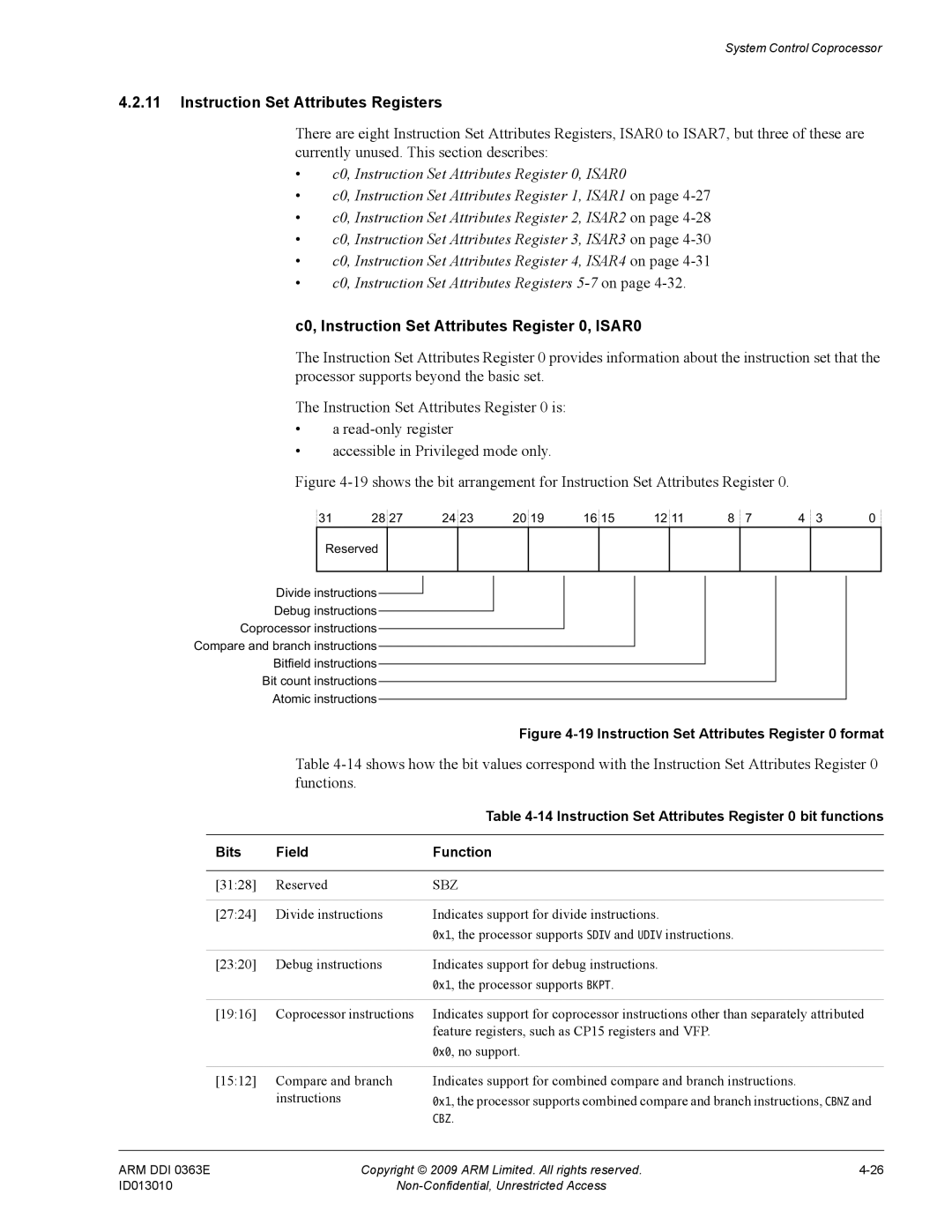
7shows the arrangement of bits in the register
Bits Field Function
3 c0, Cache Type Register
Main ID Register bit functions
Cache Type Register bit functions Bits Field Function
To access the Cache Type Register, read CP15 with
4 c0, TCM Type Register
TCM Type Register bit functions Bits Field Function
5 c0, MPU Type Register
To access the TCM Type Register, read CP15 with
To access the MPU Type Register, read CP15 with
TCM Type Register bit functions
6 c0, Multiprocessor ID Register
Processor Feature Registers
C0, Processor Feature Register 0, PFR0
Processor Feature Register 0 bit functions
To access the Processor Feature Register 0 read CP15 with
C0, Processor Feature Register 1, PFR1
Processor Feature Register 1 bit functions
Debug Feature Register 0 bit functions
To access the Processor Feature Register 1 read CP15 with
8 c0, Debug Feature Register
3124 Reserved
Memory Model Feature Registers
To access the Debug Feature Register 0 read CP15 with
9 c0, Auxiliary Feature Register
C0, Memory Model Feature Register 0, MMFR0
C0, Memory Model Feature Register 1, MMFR1
10 Memory Model Feature Register 0 bit functions
16 Memory Model Feature Register 1 format
11 Memory Model Feature Register 1 bit functions
DMB
C0, Memory Model Feature Register 2, MMFR2
WFI
3112 Reserved
C0, Memory Model Feature Register 3, MMFR3
13 Memory Model Feature Register 3 bit functions
14 Instruction Set Attributes Register 0 bit functions
Instruction Set Attributes Registers
C0, Instruction Set Attributes Register 0, ISAR0
C0, Instruction Set Attributes Register 1, ISAR1
20 Instruction Set Attributes Register 1 format
Indicates support for if then instructions
C0, Instruction Set Attributes Register 2, ISAR2
ITE
Indicates support for PSR instructions
16 Instruction Set Attributes Register 2 bit functions
PSR
Thumb instruction sets
C0, Instruction Set Attributes Register 3, ISAR3
17 Instruction Set Attributes Register 3 bit functions
C0, Instruction Set Attributes Register 4, ISAR4
23 Instruction Set Attributes Register 4 format
18 Instruction Set Attributes Register 4 bit functions
C0, Instruction Set Attributes Registers
12 c0, Current Cache Size Identification Register
4KB
8KB
13 c0, Current Cache Level ID Register
3130 Reserved
14 c0, Cache Size Selection Register
15 c1, System Control Register
TRE
23 System Control Register bit functions
AFE
Nmfi
= data caching enabled
Enables L1 data cache
= data caching disabled. This is the reset value
= strict alignment fault checking enabled
24 Auxiliary Control Register bit functions
Auxiliary Control Registers
C1, Auxiliary Control Register
Dilsm
Axiscen
Axiscuen
Deolp
Dlfo
Rsdis
Dbwr
Dnch
C15, Secondary Auxiliary Control Register
25 Secondary Auxiliary Control Register bit functions
OFC
Doofmacs
IXC
UFC
Primary input RMWENRAM0 defines the reset value
17 c1, Coprocessor Access Register
Primary input RMWENRAM1 defines the reset value
Atcmecc
All other encodings for these FSR bits are Reserved
Fault Status and Address Registers
C5, Data Fault Status Register
To use the Dfsr read or write CP15 with
C5, Instruction Fault Status Register
28 Data Fault Status Register bit functions
There are two auxiliary fault status registers
To access the Ifsr read or write CP15 with
C5, Auxiliary Fault Status Registers
29 Instruction Fault Status Register bit functions
= Atcm
C6, Data Fault Address Register
30 Adfsr and Aifsr bit functions
= Btcm
C6, Instruction Fault Address Register
19 c6, MPU memory region programming registers
C6, MPU Region Size and Enable Registers
C6, MPU Region Base Address Registers
32 Region Size Register bit functions
C6, MPU Region Access Control Registers
158 Sub-region disable
33 MPU Region Access Control Register bit functions
TEX
UNP
34 Access data permission bit encoding
C6, MPU Memory Region Number Register
35 MPU Memory Region Number Register bit functions
Point of Unification PoU
Cache operations
Point of Coherency PoC
Invalidate and clean operations
Set and Way format
36 Functional bits of c7 for Set and Way
37shows the cache sizes and the resultant bit range for Set
Address format
37 Widths of the set field for L1 cache sizes Size Set
21 c9, Btcm Region Register
Data Synchronization Barrier operation
Data Memory Barrier operation
38 Functional bits of c7 for address format Bits Field
39 Btcm Region Register bit functions
To access the Btcm Region Register, read or write CP15 with
22 c9, Atcm Region Register
24 c11, Slave Port Control Register
To access the Atcm Region Register, read or write CP15 with
23 c9, TCM Selection Register
40 Atcm Region Register bit functions
312 Reserved
25 c13, Fcse PID Register
26 c13, Context ID Register
RAZ/UNP
27 c13, Thread and Process ID Registers
Ccnt overflow IRQ request
C15, nVAL IRQ Enable Set Register
Validation Registers
C15, nVAL FIQ Enable Set Register
Ccnt overflow FIQ request
Ccnt overflow reset request
C15, nVAL Reset Enable Set Register
C15, nVAL Debug Request Enable Set Register
C15, nVAL IRQ Enable Clear Register
Ccnt overflow debug request
C15, nVAL FIQ Enable Clear Register
48 nVAL IRQ Enable Clear Register format
C15, nVAL Reset Enable Clear Register
303 Reserved UNP or Sbzp
C15, nVAL Debug Request Enable Clear Register
51 nVAL Debug Request Enable Clear Register format
318 Reserved
C15, nVAL Cache Size Override Register
50 nVAL Cache Size Override Register
B0000 4kB B0001 8kB B0011 16kB B0111 32kB B1111 64kB
Correctable Fault Location Register
53 Correctable Fault Location Register cache
52 Correctable Fault Location Register cache
C15, Build Options 1 Register
To access the Build Options 1 Register, write CP15 with
Build Options Registers
C15, Build Options 2 Register
Nodcache
55 Build Options 2 Register
Noicache
Atcmes
Nofpu
Btcmes
Noie
Nompu
Dcachees
To access the Build Options 2 Register, write CP15 with
Noharderrorcach
Axibusparity
Prefetch Unit
About the prefetch unit
Branch prediction
Disabling program flow prediction
Incorrect predictions and correction
Configuring the branch predictor
Branch predictor
Return stack
Events and Performance Monitor
Event bus interface bit functions
Bit position Update Value
About the events
Event
ETMEXTOUT0
ETMEXTOUT1
But with different attributes Dual issue case a branch
Non-cacheable access on AXI master bus
Instruction cache access
Dual issue case B1, B2, F2 load/store, F2D
TCM correctable ECC error reported by load/store unit Yes
TCM correctable ECC error reported by prefetch unit Yes
About the PMU
1 c9, Performance Monitor Control Register
Performance monitoring registers
Performance monitoring registers are described
2shows how the bit values correspond with the Pmnc Register
2 c9, Count Enable Set Register
Pmnc Register bit functions
Cntens Register bit functions Bits Field Function
To access the Cntens Register, read or write CP15 with
3 c9, Count Enable Clear Register
4 c9, Overflow Flag Status Register
To access the Cntenc Register, read or write CP15 with
Cycle counter enable clear
Cntenc Register bit functions Bits Field Function
5 c9, Software Increment Register
To access the Flag Register, read or write CP15 with
5shows how the bit values correspond with the Flag Register
Swincr Register bit functions Bits Field Function
To access the Swincr Register, read or write CP15 with
6 c9, Performance Counter Selection Register
313 Reserved RAZ on reads, Sbzp on writes Increment Counter
SEL
7 c9, Cycle Count Register
8 c9, Event Selection Register
To access the EVTSELx Register, read or write CP15 with
EVTSELx Register bit functions
Useren Register bit functions
10 c9, User Enable Register
9 c9, Performance Monitor Count Registers
10 Intens Register bit functions Bits Field Function
11 c9, Interrupt Enable Set Register
Ccnt overflow interrupt enable
11 Intenc Register bit functions Bits Field Function
12 c9, Interrupt Enable Clear Register
Ccnt overflow interrupt enable bit
To access the Intenc Register, read or write CP15 with
Event bus interface
Use of the event bus and counters
Memory Protection Unit
MPU faults on
MPU software-accessible registers on
True
Default memory map
About the MPU
Region size
Memory regions
Region base address
Subregions
Overlapping regions
Region access permissions
Region attributes
Region
Example of using regions that overlap
Example of using subregions
Background regions
TCM regions
Using memory types
Memory types
ARM DDI 0363E
Region attributes
TEX20, C, and B encodings Description Memory Type Shareable?
Cacheable memory policies
1BB
Following code is an example of disabling the MPU
On page 7-2shows the default memory map
MPU interaction with memory system
Background fault
MPU faults
Background fault Permission fault Alignment fault
Permission fault
MPU software-accessible registers
On page 4-5shows the CP15 registers that control the MPU
Level One Memory System
About the L1 memory system
L1 memory system block diagram
Parity
About the error detection and correction schemes
Parity Bit ECC on
Bit ECC
Error checking and correction
Hard errors
Read-Modify-Write
Correct-and-retry
Error correction
Correct inline
Classes of fault that can occur are
Fault handling
Faults
MPU faults
TCM external faults
External faults
Cache and TCM parity and ECC errors
Precise and imprecise aborts
Fault status information
Debug events
Abort exceptions
Usage models
Precise abort exceptions
Imprecise abort exceptions
AXI
Correctable errors
Types of aborts Conditions Source Precise Fatal
ARM DDI 0363E
About the TCMs
TCM attributes and permissions
Handling TCM parity errors on Handling TCM ECC errors on
Atcm and Btcm configuration
TCM internal error detection and correction
TCM arbitration
Handling TCM parity errors
Handling TCM ECC errors
TCM port protocol
External TCM errors
TCM initialization
AXI slave interfaces for TCMs
About the caches
Store buffer
Store buffer behavior
Cache maintenance operations
Store buffer merging
Store buffer draining
Cache error detection and correction
Error build options
Cache parity error behavior Value Behavior
Address decoder faults
Handling cache parity errors
Handling cache ECC errors
Cache ECC error behavior Value Behavior
Errors on data cache write
Errors on instruction cache read
Errors on data cache read
Errors on evictions
Invalidate all instruction cache
Clean data cache by set/way
Dirty RAM on Data RAM on
Cache RAM organization
Tag RAM
Tag RAM
Cache sizes and tag RAM organization Tag RAM organization
Dirty RAM
Data RAM
Organization of a dirty RAM line
Nonsequential read operation performed with one RAM access
Data RAM sizes without parity or ECC implemented
13 Data cache RAM bits, with parity Description
Following code is an example of enabling caches
Cache interaction with memory system
Disabling or enabling all of the caches
15 Data cache data RAM sizes with ECC Cache size Data RAMs
Disabling or enabling data cache
Disabling or enabling error checking
Disabling or enabling instruction cache
MCR p15 R0, c1 Write System Control Register
Internal exclusive monitor
Memory types and L1 memory system behavior
Instruction-cache error events
Error detection events
TCM error events
Data-cache error events
ARM DDI 0363E
Level Two Interface
About the L2 interface
Attribute Value Comments
AXI master interface
1shows the AXI master interface attributes
Outstanding write accesses with the same ID
Identifiers for AXI bus accesses
Outstanding write/read access on different IDs
Write response
Arcachem and Awcachem encodings Encoding a Meaning
Eviction buffer
Memory attributes
Aruserm and Awuserm encodings
Memory system implications for AXI accesses
Linefills on
AXI master interface transfers
Strongly Ordered and Device transactions on
Non-cacheable Ldrb
Restrictions on AXI transfers
Strongly Ordered and Device transactions
Address20
LDR or LDM that transfers one register
Ldrh from Strongly Ordered or Device memory Address30
LDM that transfers five registers
LDM5, Strongly Ordered or Device memory Address40
Strb to Strongly Ordered or Device memory Address40
Strh to Strongly Ordered or Device memory Address20
First Wstrbm
STR or STM of one register
STM of seven registers
Non-cacheable reads
Linefills
Cache line write-back eviction
14 Ldrh from Non-cacheable Normal memory Address20
15 LDR or LDM1 from Non-cacheable Normal memory Address20
Non-cacheable or write-through writes
AXI transaction splitting
Normal write merging
20 AXI transaction splitting, data in two cache lines
Example 9-1 Write merging
ARM DDI 0363E
AXI slave interface
AXI slave interface for cache RAMs
AXI slave control
TCM parity and ECC support
Cache parity and ECC support
AXI slave characteristics
25 AXI slave interface attributes
Enabling or disabling AXI slave accesses
26 RAM region decode AxUSERS bit One-hot RAM select
Accessing RAMs using the AXI slave interface
TCM RAM access on Cache RAM access on
27 TCM chip-select decode Btcm ports
TCM RAM access
ARADDRSMSB, see Table
RAM selected
This section contains the following
Cache RAM access
Memory map when accessing the cache RAMs
31 Cache data RAM bank/address decode Inputs ARADDRS1815
Data RAM access
0010 Bank 0100 1000
0001 Bank 0010 0100 1000
34 Data format, instruction cache, with ECC
35 Data format, data cache, with ECC Data bit Description
Tag RAM access
ARM DDI 0363E
Dirty RAM access
43 Dirty register format, with ECC Data bit Description
Other examples of accessing cache RAMs
ARADDRS1815 = 4b1111
Power Control
About power control on Power management on
About power control
Dormant mode
Run mode
Standby mode
Shutdown mode
Communication to the Power Management Controller
Debug
Debug state on Cache debug on
Debug host
Debug systems
Debug host Protocol converter Debug target
Protocol converter
Monitor debug-mode debugging
About the debug unit
Halting debug-mode debugging
Programming the debug unit
All other state information associated with the debug unit
Coprocessor registers
11.3.2 CP14 access permissions
Debug register interface
Coprocessor registers summary
Instruction Mnemonic Description
Offset Register Access Mnemonic Description Hex Number
Memory-mapped registers
Debug memory-mapped registers
Memory addresses for breakpoints and watchpoints
APB port access permissions
Power domains
Effects of resets on debug registers
Privilege of memory access permission
Other Debug registers
External debug interface access permissions Registers
Lock
Other registers
6shows the CP14 debug register map
Accessing debug registers
Debug register descriptions
11.4.2 CP14 c0, Debug ID Register
BRP
Debug ID Register functions
WRP
To use the Debug ROM Address Register, read CP14 c0 with
To use the Debug ID Register, read CP14 c0 with
11.4.3 CP14 c0, Debug ROM Address Register
11.4.4 CP14 c0, Debug Self Address Offset Register
Debug Self Address Offset Register format
Debug Self Address Offset Register functions
11.4.5 CP14 c1, Debug Status and Control Register
10 Debug Status and Control Register functions
Flag is set to 1 on entry to debug state
ARM
Execute ARM instruction enable bit
= disabled, this is the reset value
DTR access mode
MOE
Data Transfer Register
Vector Catch Register
Watchpoint Fault Address Register
12 Watchpoint Fault Address Register functions
Reserved RAZ
SVC
Instruction Transfer Register
Bits Field Reset Description Value
Debug State Cache Control Register
14 Debug State Cache Control Register functions
315 Reserved
Debug Run Control Register
15 Debug Run Control Register functions
Breakpoint Value Registers
Breakpoint Control Registers
17 Breakpoint Control Registers functions
18 Meaning of BVR bits
+0 is accessed
Corresponding instruction address breakpoint
BVR2220 Meaning
19 Watchpoint Value Registers functions Bits Description
Watchpoint Value Registers
Watchpoint Control Registers
11 Watchpoint Control Registers format
20 Watchpoint Control Registers functions
Accessed
Operating System Lock Status Register
Authentication Status Register
21 OS Lock Status Register functions
= Dbgnopwrdwn is LOW. This is the reset value
Device Power-down and Reset Control Register
Device Power-down and Reset Status Register
23 Prcr functions
15 Prsr format
24 Prsr functions
Management registers
Processor ID Registers
27 Claim Tag Set Register functions Bits Field Function
Claim Registers
Claim Tag Set Register
Claim Tag Clear Register
Lock Access Register
318 Reserved RAZ or Sbzp Claim tag clear Reset value is
Lock Status Register
30 Device Type Register functions
Device Type Register
Debug Identification Registers
33 Peripheral ID Register 0 functions
32 Fields in the Peripheral Identification Registers
Field Size Description
Bits Value Description
36 Peripheral ID Register 3 functions
34 Peripheral ID Register 1 functions
35 Peripheral ID Register 2 functions
37 Peripheral ID Register 4 functions
1021
1020
Component Identification Register
1022
Debug events
Software debug event
Debug event priority
Halting debug event
Behavior of the processor on debug events
Watchpoint debug events
Debug exception
Effect of debug exceptions on CP15 registers and Wfar
40shows the values in the link register after exceptions
Following sections describe
Four CP15 registers that record abort information are
Avoiding unrecoverable states
Entering debug state
Debug state
Privilege on
41 Read PC value after debug state entry
Behavior of the PC and Cpsr in debug state
41 Read PC value after debug state entry Debug event
Writing to the Cpsr in debug state
Accessing registers and memory
Executing instructions in debug state
Privilege
Effects of debug events on processor registers
Coprocessor instructions
Effect of debug state on non-invasive debug
Exceptions in debug state
Imprecise Data Aborts on entry and exit from debug state
Precise Data abort
Imprecise Data Abort
Leaving debug state
Sets the DSCR1 core restarted flag to
Cache pollution in debug state
Cache debug
This section describes cache debug. It consists
Cache coherency in debug state
This section describes the miscellaneous debug signals
APB signals
Miscellaneous debug signals
External debug interface
42 Authentication signal restrictions Dbgen a
Authentication signals
Changing the authentication signals
Non-invasive debug permitted
Issue an Instruction Synchronization Barrier ISB instruction
Using the debug functionality
Example 11-1 Executing an ARM instruction through the ITR
Rules for accessing the DCC
Debug communications channel
Example 11-5shows the code for host-to-target data transfer
Software access to the DCC
Debugger access to the DCC
Example 11-4 Target to host data transfer host end
Programming simple breakpoints and the byte address select
Programming breakpoints and watchpoints
This section describes the following operations
Example 11-6 Polling the DCC host end
Setting a simple aligned watchpoint
Example 11-7 Setting a simple breakpoint
Setting a simple unaligned watchpoint
Example 11-8 Setting a simple aligned watchpoint
Single-stepping
Example 11-9 Setting a simple unaligned watchpoint
45shows some examples
Not required
Example 11-11 Entering debug state
Debug state entry
Example 11-10 Single-stepping off an instruction
Debug state exit
Example 11-12 Leaving debug state
Reading and writing registers through the DCC
Accessing registers and memory in debug state
This section describes the following
Example 11-13 Reading an ARM register
Reading the Cpsr in debug state
Reading the PC in debug state
Example 11-15shows the code to read the PC
Example 11-16shows the code for reading the Cpsr
Example 11-18shows the code for reading a byte of memory
Example 11-19 Checking for an abort after memory access
Reading memory
Example 11-17 Writing the Cpsr
Example 11-20 Reading a block of bytes of memory
Example 11-21 Reading a word of memory
Example 11-24 Writing registers in stall mode
Example 11-22 Changing the DTR access mode
Example 11-23 Reading registers in stall mode
Fast register read/write
Fast memory read/write
Example 11-25 Reading a block of words of memory
Accessing coprocessor registers
Example 11-27 Reading a coprocessor register
11-70
Emulating power down
Debugging systems with energy management capabilities
11-72
FPU Programmer’s Model
About the VFPv3-D16 architecture
About the FPU programmer’s model
FPU functionality
General-purpose registers
FPU views of the register bank
1shows the VFP system registers in the Cortex-R4F FPU
System registers
VFPv3 architecture describes the following system registers
Mvfr registers are privileged access only
All hardware ID information is privileged access only
Fpsid is privileged access only
This is a change in VFPv3 compared to VFPv2
DNM
Floating-Point Status and Control Register, Fpscr
Fpscr Register bit functions
Rmode
IDE RAZ
Floating-Point Exception Register, Fpexc
LEN
DNM IXE RAZ UFE OFE DZE IOE IDC
DEX
Media and VFP Feature Registers, MVFR0 and MVFR1
Floating-Point Exception Register bit functions
MVFR0 Register bit functions
MVFR1 Register bit functions
Full denormal arithmetic supported for VFP
Flush-to-zero mode
Full-compliance mode Flush-to-zero mode Default NaN mode
Full-compliance mode
Default NaN mode
Ieee 754 standard implementation choices
Compliance with the Ieee 754 standard
Complete implementation of the Ieee 754 standard
NaN handling
QNaN and SNaN handling
Comparisons
Underflow
CDP
Exceptions
Integration Test Registers
About Integration Test Registers
Software access using APB
Programming and reading Integration Test Registers
Itmiscout
Register Itctrl
Itetmif
Itmiscin
1110
Processor integration testing
1312
Using the Integration Test Registers
Performing integration testing
Itetmif Register ETM interface
Itetmif Register bit assignments Bits Name Function
Itmiscout Register bit assignments Bits Name Function
Itmiscout Register Miscellaneous Outputs
Itmiscin Register Miscellaneous Inputs
Dbgrestart
Integration Mode Control Register Itctrl
Bits Name Function
Etmextout
RAZ/SBZP
Bits Access Reset value Name Function
7shows the fields of the Itctrl Register
Intmode
Cycle Timings and Interlock Behavior
Multiplies on Divide on Branches on
Dual issue on
About cycle timings and interlock behavior
Instruction execution overview
Conditional instructions
Following sequence where R1 is a Late Reg takes two cycles
Flag-setting instructions
Definition of terms
Assembler language syntax
Takes two cycles because there are no register dependencies
Register interlock examples
Instruction Behavior Sequence
Takes three cycles because of the result latency of R1
Cycle counts if destination is the PC
Data processing instructions
Cycle counts if destination is not PC
Register controlled shifts
Example interlocks
Shifter
QADD, QDADD, QSUB, and Qdsub instructions
Media data-processing
SEL
Result of the USAD8 instruction
Sum of Absolute Differences SAD
Instruction sequence Behavior
USAD8 instruction
Multiplies
Umlals
14-13
Divide
Example instruction Cycles Memory Comments
Branches
10 Branch instruction cycle timing behavior
All MRS instructions
Mode changing
Processor state updating instructions
All MSR instructions to the Spsr
Single load and store instructions
13shows the cycle timing behavior for loads to the PC
Example instruction Cycles Memory Result Comments Latency
Base register update
13 Cycle timing behavior for loads to the PC
14-19
Register offset, then 3-issue cycles
Load and Store Double instructions
Load and Store Multiple instructions
Write-back
Return stack prediction
Load Multiples, where the PC is in the register list
Correct condition prediction and correct
Correct condition prediction and incorrect
14-23
RFE and SRS instructions
Synchronization instructions
Clrex
Coprocessor instructions
Some instructions such as cache operations take more cycles
SVC formerly SWI
Prefetch Abort Undefined Instruction
Miscellaneous instructions
Serializing
Floating-point register transfer instructions
Blocking and serializing
Not aligned
Floating-point load/store instructions
Bit aligned address
2,2
2,3
4,5
Floating-point single-precision data processing instructions
Floating-point double-precision data processing instructions
Dual issue rules
Dual issue
Dual issue rules Permitted combinations on
28 Permitted instruction combinations
Dual issue First instruction Second instruction Case
Permitted combinations
Multiply-accumulate instructionso
Case F2stb
Any single-precision CDPi, excluding
Case F2Db
AC Characteristics
Processor timing on Processor timing parameters on
Processor timing
Clock uncertainty 10%
Processor timing parameters
Input port timing parameters
Clock uncertainty 50%
Clock uncertainty 60%
3shows the timing parameters for the interrupt input ports
4shows the input timing parameters for the AXI master port
5shows the input timing parameters for the AXI slave port
Rreadys
6shows the input timing parameters for the debug input ports
7shows the input timing parameters for the ETM input ports
Clock uncertainty 40%
8shows the timing parameters for the test input ports
Clock uncertainty 65%
Output ports timing parameters
11shows the timing parameters for the interrupt output ports
13shows the timing parameters for the AXI slave output ports
Write response channel Clock uncertainty 60%
BRESPS10
16shows the timing parameters for the test output ports
Clock uncertainty 45%
18shows the timing parameters for the FPU output signals
Fpidc
15-13
Processor Signal Descriptions
FPU signals on page A-23
From any clock
About the processor signal descriptions
Any
Signal Direction Clocking Description
Global signals
Table A-1 Global signals
Table A-2 Configuration signals
Configuration signals
Table A-2shows the processor configuration signals
Information
Tie LOW for even parity
Tie High for odd parity
RMWENRAM10b
Interrupt signals, including VIC interface signals
AXI master port
L2 interface signals
Table A-4 AXI master port signals for the L2 interface
Identification tag for the read address group of signals
Identification tag for the write data group of signals
Identification tag for the write response signal
Protection signals provide addition information about a bus
Table A-6 AXI slave port signals for the L2 interface
AXI master port error detection signals
Table A-5 AXI master port error detection signals
AXI slave port
Protection information, privileged/normal access. ARPROT0
Protection information, privileged/normal access. AWPROT0
AXI specification
One to 16. a four bit binary value minus one determines
Standard AXI specification
AXI slave port error detection signals
ATCM, one hot. AWUSERS30 signal is not part
Table A-7 AXI slave port error detection signals
Table A-9shows the B0TCM port signals
TCM interface signals
Table A-8shows the Atcm port signals
= DMA
Table A-10shows the B1TCM port signals
Table A-10 B1TCM port signals
Write data for B1TCM data RAM
B1TCM RAM access is sequential
Address for B1TCM data RAM
Write parity or ECC code for B1TCM
Table A-11 Dual core interface signals
Dual core interface signals
Table A-11shows the dual redundant core interface signals
Table A-12 Debug interface signals
Debug interface signals
Table A-13shows the debug miscellaneous signals
Input Tie-off Debug self-address offset
Table A-13 Debug miscellaneous signals
Input Tie-off Debug ROM physical address valid
Input Tie-off Debug self-address offset valid
Table A-14 ETM interface signals
ETM interface signals
Table A-14shows the ETM interface signals
Table A-15 Test signals
Test signals
Table A-15shows the test signals
Mbist signals
Table A-16shows the Mbist signals
Validation signals
Table A-17shows the validation signals
FPU signals
Table A-18 FPU signals
ECC Schemes
ECC scheme selection guidelines on page B-2
ECC scheme selection guidelines
Clarified byte-invariant big-endian format
NCPUHALT removed from timing diagram Added sections
Revisions
Clarified little-endian format
Table C-1 Differences between issue B and issue C
Change Location
Table C-2 Differences between issue C and issue D
No technical changes
See also Data Abort, External Abort and Prefetch Abort
Glossary
Abort, and an internal or External Abort
Base register write-back
That are divisible by four and two respectively
See also Advanced High-performance Bus
See Advanced High-performance Bus
See Advanced Microcontroller Bus Architecture
Active write transaction
Active read transaction
Active transfer
Completed transfer
Write ID capability
Read ID width
Read issuing capability
Write ID width
See also Burst
See also Beat
See also Word-invariant
Accesses are expected to be word-aligned
Accessed in parallel during a cache look-up
Bus
See also Dirty
See also Clean
See Embedded Trace Macrocell
Option chosen does not affect software compatibility
An instruction that is architecturally Undefined
By individual implementations
Precision and the fraction is all zeros
See Cold reset
Serviced while normal program execution is suspended
See also Halt mode
Result of attempting to access invalid instruction memory
See Should Be Zero
Or equal to 1 and is not restricted to being a power of two
See Should Be One
See Boundary scan chain
Destination precision
See Debug test access port
Increment of +2
User trap handler is executed
Processor-specific. a victim is also known as a cast out
Expected behavior for an unaligned access
Bit for the exception is set
A processor
Cache terminology diagram