Product Guide
Page
Preface
Page
Table of Contents
Design Architecture
Table of Contents M2488 Product Guide
Scsi Messages
Tape Unit Scsi Commands
Table of Contents
Receive Diagnostic Results Factory Mode
Receive Diagnostic Results Check Condition
Send Diagnostic Factory Mode Check
Tape Unit Parameters
Media Changer Scsi Commands
MC Medium Changer INQUIRY/CHANGE Definition
Additional Command Information on Medium Changer
Tape Processing
Maintenance and Servicing
Xii C144-E019-03EN
Parts Replacement Catalog
Parameter List Diag Result Data
M2488 Product Guide List of Figures
List of Figures
Top Cover
List of Figures M2488 Product Guide
M2488 Product Guide List of Tables
List of Tables
List of Tables M2488 Product Guide
C144-E019-03EN Xix
List of Tables
C144-E019-03EN Xxi
Xxii C144-E019-03EN
C144-E019-03EN Xxiii
Xxiv C144-E019-03EN
Preparing the M2488 and ITS Optional Equipment
Chapter Installation Instructions
Configurations
Introduction
Rack-mount Configurations
Installation Instructions M2488 Product Guide
Rack-mount
Desktop
Desktop Configurations
IPM
Unpack the M2488 Tape Drive
Unpacking Instructions
ACL
Unpack the Automatic Cartridge Loader
Facl
Unpack the Flush-mounted Automatic Cartridge Loader
Inspect the Facl
Equipment Inspection
Inspect the M2488 Tape Drive
Inspect the ACL
FACL?
Assembly Instructions
IPM
Interface Personality Module Installation
Step Action
See Figure
Cable and Power Connections
Drive with ACL Attached 5-Cartridge Magazine
Desktop Installation Instructions
Tools Required
Tape Drive Only
Attaching Bases
Drive with ACL Attached 10-Cartridge Magazine
Stability Brackets
Drive Positioning
M2488 with Facl in Desktop Model
Drive with Facl Attached
10. Attach to Bottom Base
11. Desktop Model Top Covers
12. Desktop Model Rear Cover
5.2.1 Inner Cover Mounted to Mounting Tray
Rack-Mount Installation
5.2 Adjust the Guide Plate
5.1 Tools Required
Attach Mounting Tray
13. Guide Plate Installation Screw Plate Mounting
14 -inch Rack-mount Kit Installation
15. Bracket Adjustment
Adjust the Brackets
16. M2488 Tray Mounting
17. M2488 with ACL Tray Mounting
19. Facl Face Plate
Equipment and Tools Required for ACL Installation
Installation of the Automatic Cartridge Loader
Equipment Part Number Quantity Description ACL
20. Prepare the M2488 Tape Drive
Prepare the M2488 Tape Drive
21. Prepare the ACL
Prepare the ACL
22. Connect the M2488 and the ACL Base
Connect the M2488 and the ACL
23. Attach Operator Panel Cable to ACL Base
Excess cable
25. Replace Covers
Equipment and Tools Required for Facl Installation
Installation of the Flush-mount Automatic Cartridge Loader
Equipment Part Number Quantity Description Facl
26. Prepare the M2488 Tape Drive
27. Prepare the Facl
Prepare the Facl
28. Facl Rear Connect the M2488 and the Facl
29. Connect the M2488 and the Facl
31. Replace Top Covers
Preparation for USE
Page
2OPERATION of the M2488
Chapter Design Architecture
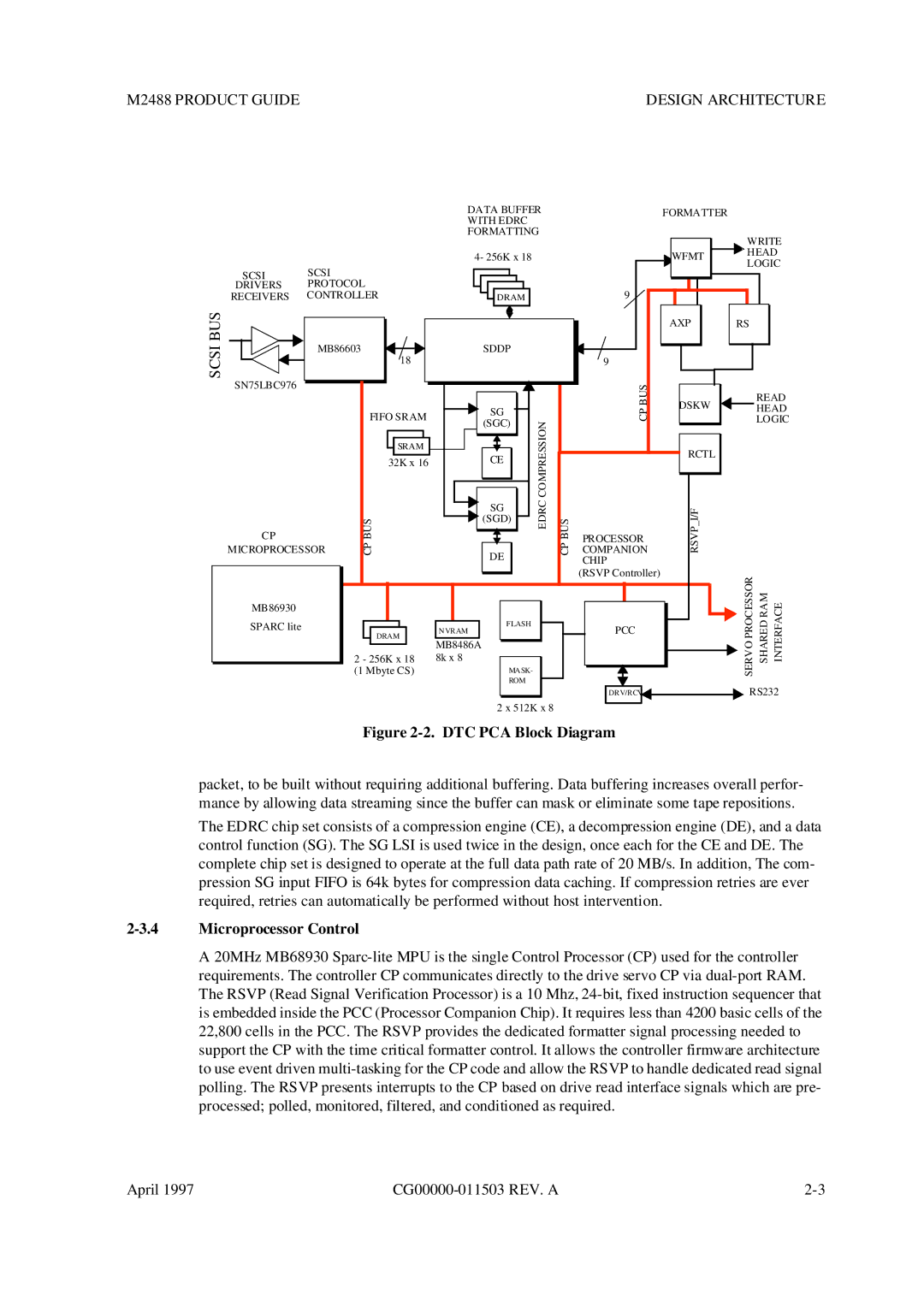
Data Path
Erdc Compression Feature
Operation of the Magnetic Tape Controller MTC
Design Architecture M2488 Product Guide
Microprocessor Control
M2488 Product Guide Design Architecture Scsi BUS
Firmware
Operation of the Magnetic Tape Unit MTU
Airless Tape Path
PCA-OP
PCA-DVL
CG00000-011503 REV. a April
M2488 Scsi Messages
Chapter Scsi Messages
M2488 Tape and Medium Changer Scsi Messages
M2488 Product Guidescsi Messages
Abort code 06h
BUS Device Reset code 0Ch
Command Complete code 00h
Scsi Messages M2488 Product Guide
Code Message Length Bytes
M2488 Product Guide Scsi Messages
Extended Message Format code 01h
Synchronous Data Transfer Request Sdtr
Supported Scsi transfer rates are listed in Appendix G
Bits Bytes
Wide Data Transfer Request Wdtr
Scsi Messages M2488 Product Guide
Ignore Wide Residue code 23h
Identify code 80h-FFh
Byte Value Description
Message Parity Error code 09h
Initiator Detected Error code 05h
Linked Command Complete code 0Ah
Linked Command Complete with Flag code 0Bh
No Operation code 08h
Restore Pointers code 03h
Save Data Pointer code 02h
Scsi BUS Status
Reservation Conflict Status
Page
Chapter
Tape Unit Scsi Commands
Logical Units and Scsi IDS
Command Description Paragraph Code
M2488 Tape Scsi Commands
Tape Unit Scsi Commands M2488 Product Guide
M2488 Scsi Commands
M2488 Product Guide Tape Unit Scsi Commands
CDB Field Description
Command Description Block Format
Field Description
Bits Bytes LUN
Change Definition command 40h
Change Definition CDB Description
Change Definition Field Description
Change Definition Changes
Definition Parameter Description
Value Meaning of Definition Parameter
Change Definition Sense Keys
Change Definition Check Condition Status
Sense KEY Condition Description
Display Field Description 11h
Display CDB Description 11h
Display Parameter 11h
Display Data 11h
Display Parameter Field Description 11h
Space
Display Data
Display Sense Keys 11h
Display Mode Selection Bits 11h
Qualifier Description
10. Display Field Description 10h
Display CDB Description 10h
LUN
Display Data 10h
11. Display Format Control Byte Description 10h
12. Display Parameter 10h
4.3 Display Sense Keys 10h
13. Display Mode Selection Bits 10h
Immed BIT Long BIT Action Taken
Erase command 19h
Erase CDB Description
14. Erase Field Description
Not Ready
Erase Sense Keys
Data Protect
Aborted Command
Evpd
Inquiry command 12h
Inquiry CDB Description
15. Inquiry Field Description
Inquiry Data
16. Evpd Bit
17. Supported VPD Page Codes
Inquiry Check Condition Status
18. Inquiry Data Format
19. Inquiry Data Format Field Description
Inquiry Data Format Field Description
LUN Peripheral Description Qualifier Device Type
20. Peripheral Qualifiers
21. Peripheral Device Type
Code Description
MTU Fujitsu
23. Default Vendor and Product Identification Fields
Inquiry Sense Keys
LUN Vendor ID Controller LUN Product ID
7.1LOAD Unload CDB Description
Load Unload command 1Bh
24. Load Unload Field Description
Load Unload Check Condition Status
Medium Changer
GAL Request
Load Unload Sense Keys
LSB
Locate command 2Bh
Locate CDB Description
25. Locate Field Description
26. Block ID Format
Locate Field Description
27. Block ID Format Field Description
28. Format Mode Values
Format Code Value
Locate Sense Keys
Locate Check Condition Status
LOG Select Check Condition Status
LOG Select command 4Ch
LOG Select CDB Description
29. LOG Select Field Description
LOG Sense CDB Description
LOG Sense command 4Dh
30. LOG Sense Field Description
Field in CDB
BUS Device Reset
31. Page Codes
LOG Sense Operation
32. Log Page Format
LOG Sense Parameters
34. LOG Parameter Field Description
33. Log Parameter Format
ETC=0
36. Log Sense Page 00h, Supported Log Pages
Default Bytes Value
Write Errors Detected by Firmware
37. Log Sense Page 02h, Error Counter Page Write
Bits Default Bytes Value
Write Errors Recovered by ECC
Total Tapemarks Written
Bits Default Bytes Value Bytes Transferred from Initiator
TMC=0
Total Write Blocks
Read Errors Detected by Firmware
38. Log Sense Page 03h, Error Counter Page Read
Bits Default Bytes Value Erase Gaps DUE to Retry
Read Errors Recovered by ECC
Total Read Blocks That Were Recorded in Edrc Format
Total Errors Corrected
Total Read Forward Bytes
Bytes Transferred to Initiator
Read Retries
Total Read Blocks That Were not Recorded in Edrc Format
39. Log Sense Page 0Ch, Sequential-Access Device
Error Statistics by Track
40. Log Sense Page 31h, Track Error Statistics
Log Sense Page 31h, Track Error Statistics
136
175
LOG Sense Sense Keys
Loop Write to Read CDB Description
Loop Write to Read command C1h
41. Loop Write to Read Field Description
Loop Write to Read Sense Keys
Hardware Error
Volume Overflow
Loop Write to Read Check Condition Status
Byte BIT Valu Description
Mode Select command 15h
Mode Select CDB Description
42. Mode Select Field Description
43. Mode Select Parameter List Format
Mode Select Data
45. Mode Select Parameter Header Field Description
47. Block Descriptor
46. Buffered Mode Values
Buffered Description Mode
Block Descriptor
Descriptor 49. Page Descriptors
Block Descriptor Field Description
50. Page Descriptor Field Description
Mode Select Sense Keys
Mode Sense CDB Description
Mode Sense command 1Ah
51. Mode Sense Field Description
52. PC Field
Mode Sense Data
Mode Sense Data Header 53. Mode Sense Data Header
Bits Default Bytes
55. Buffered Mode Description
54. Mode Sense Data Header Field Description
56. Block Descriptor
57. Mode Select Parameter Header Field Description
Descriptor 58. Page Descriptors
Initiator Setup
Mode Settings
59. Page Descriptor Field Description
M2488 Product Guide Tape Unit Scsi Commands
Mode Sense Sense Keys
Sili
Read command 08h
Read CDB Description
60. Read Field Description
Read Check Condition Status
Fixed Sili Block Description BIT Mode
Are both set to one
No Sense
Read Sense Keys
Blank Check
Read command was aborted
62. Read Block Limits Data
Read Block Limits command 05h
Read Block Limits CDB Description
61. Read Block Limits Field Description
Read Block Limits Sense Keys
Read Buffer CDB Description
Read Buffer command 3Ch
63. Read Buffer Field Description
Byte Mode Implemented BIT
64. Read Buffer Command Mode
Vendor Unique Mode 001b and Data Mode 010b
65. Supported Buffer ID Values for Read Data Mode
67. Read/Write Nvram Descriptor buffer ID
Descriptor Mode 011b
68. Descriptor Mode Field Description
66. Read/Write Data Buffer Descriptor buffer ID
Boundary Offset Boundary Buffer Offsets
69. Offset
Read Buffer Sense Keys
17.1READ Position CDB Description
Read Position command 34h
70. Read Position Field Description
Bits Bytes BOP EOP
Read Position Return Data
MSB
Byte BIT Description
71. Read Position Return Data Description
72. Block ID Field Description
17.3 Description of Block ID Format
73. Format Codes
Read Position Sense Keys
18.1READ Reverse CDB Description
Read Reverse command 0Fh
74. Read Reverse Field Description
Invalid Field in CDB
Read Reverse Check Condition Status
Read Reverse Sense Keys
Receive Diagnostic Results CDB Description
Receive Diagnostic Results command 1Ch
75. Receive Diagnostic Results Field Description
Routine Parameter Code List Length
76. Receive Diagnostic Parameter List Length Field
79. Page 00h Supported Diagnostic Pages
Diagnostic Page Codes PF=1 in Send Diagnostic command CDB
77. Diagnostic Page Codes
78. Receive Diagnostic Results Page, General Form
81. Page 80h Field Description
Receive Diagnostic Results Check Condition Status
82. Online Diagnostic Results data Parameter List
Receive Diagnostic Results Sense Keys
Mode
Receive Diagnostic Results Factory Mode command 1Ch
Receive Diagnostic Results Factory Mode CDB Description
84. Receive Diagnostic Results Field Description
Routine Parameter Code List Length
87. Receive Diagnostic Results Page, General Form
86. Diagnostic Page Codes
88. Page 00h Supported Diagnostic Pages Factory Mode
00h Supported Diagnostic Pages Factory Mode
90. Page 80h Field Description
92. Page 81h Field Description
90-9Fh Online Diagnostic Test
95. Online Diagnostic Results data Parameter List
Receive Diagnostic Results Sense Keys
Bits Bytes Sili LUN
Recover Buffered Data command 14h
Recover Buffered Data CDB Description
97. Recover Buffered Data Field Description
Recover Buffered Data Check Condition Status
Recover Buffered Data Operation
Recover Buffered Data Sense Keys
22.1 Release Unit CDB Description
Release Unit command 17h
98. Release Unit Field Description
Release Unit Sense Keys
Release Unit Operation
Request Sense Check Condition Status
Request Sense command 03h
Request Sense CDB Description
99. Request Sense Field Description
Request Sense Sense Keys
Report Density Support CDB Description
Report Density Support command 44h
Report Density Support Data
100. Report Density Support Field Description
April CG00000-011503 REV. a 107
108 CG00000-011503 REV. a April
Ucts is discouraged since the definition of bits may vary
104. Report Density Support Data Block Field Description
110 CG00000-011503 REV. a April
Report Density Support Sense Keys
Reserve Unit CDB Description
Reserve Unit command 16h
105. Reserve Unit Field Description
Reserve Unit Operation
Reserve Unit Sense Keys
Rewind Check Condition Status
Rewind command 01h
Rewind CDB Description
106. Rewind Field Description
Rewind Sense Keys
Send Diagnostic CDB Description
Send Diagnostic command 1Dh
107. Send Diagnostic Field Description
108. Send Diagnostic CDB Field Description Overview
Send Diagnostic Field Description
Routine Selftest Devofl Unitofl Parameter Code List Length
Send Diagnostic Check Condition Status
Send Diagnostic CDB Field Description Overview
Diagnostic Pages PF=1
110. Diagnostic Page Codes
109. Send Diagnostic Page, General Form
111. Page 00h Supported Diagnostic Pages
Description of the Page Code 80h
112. Page 80h Online Diagnostic Test
113. Diagnostic Parameter List
Diagnostic Parameter List PF=0
Send Diagnostic Sense Keys
114. Send Diagnostic Factory Mode Field Description
Send Diagnostic Factory Mode command 1Dh
Send Diagnostic Factory Mode Field Description
Send Diagnostic Factory Mode Check Condition Status
Description of Page Code 00h
116. Send Diagnostic Page, General Form
117. Diagnostic Page Codes
118. Page 00h Supported Diagnostic Pages
Description of Page Code 80h
119. Page 80h Online Diagnostic Test
Description of Page Code 81h
120. Page 81h Manufacturing Online Diagnostic Test
Value of 1 is used to select Edrc Clear data transfer mode
Description of Page Codes 90-9Fh
122. Page 90-9Fh MTU Online Diagnostic Test
List
Diagnostic Parameter List PF=0
124. Diagnostic Parameter List
134 CG00000-011503 REV. a April
126. Code Field Bits
Space command 11h
Space CDB Description
125. Space Field Description
End-of-Tape Parameter
Space Check Condition Status
Filemark Parameter
End-of-Data Parameter
Space Sense Keys
Test Unit Ready Check Condition Status
Test Unit Ready command 00h
Test Unit Ready CDB Description
127. Test Unit Ready Field Description
Test Unit Ready Sense Keys
Write Check Condition Status
Write command 0Ah
Write CDB Description
128. Write Field Description
Sense Data Information Bytes
Buffered Mode
Early Warning Indication
Deferred Write Errors
Additional Information
Write Sense Keys
32.1WRITE Buffer CDB Description
Write Buffer command 3Bh
129. Write Buffer Field Description
Mode Bits Implemented Modes
130. Write Buffer Modes
Buffer ID Description Capacity
M2488 Product Guide Tape Unit Scsi Commands
Write Buffer Check Condition Status
Microcode has Been Changed
Write Buffer Sense Keys
Write Filemarks CDB Description
Write Filemarks command 10h
132. Write Filemarks Field Description
Write Filemarks Check Condition Status
133. Write Filemark Command Operations
Buffer Immed Operation Mode BIT
Buffer Block Information Field Mode
Write Filemarks Sense Keys
Blank Check Aborted Command
Scsi Reset
Command Disconnection
Page
Parameters Savable Bit All pages
Chapter Tape Unit Parameters
M2488 Product Guide Tape Unit Parameters
Codes
00 -Vendor Unique Parameter Field Description
Vendor Unique Parameter 00 Vendor Unique Parameter
Played on the op panel display
Tape Unit Parameters M2488 Product Guide
Error Recovery and Reporting Parameters
01 Error Recovery and Reporting Parameters
Error Recovery and Reporting Parameters Field Description
State of the other error recovery flags
EER PER DTE DCR Description
Valid Combinations of Error Recovery Parameters
Dtdc
Disconnect/Reconnect Control Parameters
02 Disconnect/Reconnect Parameters
02 Disconnect/Reconnect Parameters Field Description
Data Transfer Disconnect Control
Eeca
Rlec
Chronous event notification
EEG SEW
Bytes
DBR BIS
AVC Socf RBO REW
Is changed to the value specified in the active format field
10h Device Configuration Parameters Field Description
EOM
Density Code 28h
Density Code Description
7.1 M2488 Operation When Density Code 28h Is Not Configured
7.2 M2488 Operation When Density Code 28h Is Configured
When the Following is True Mode Sense will Report
Tape Unit PARAMETERSM2488 Product Guide
18. VPD Page Format
MTU INQUIRY/CHANGE Definition Vital Product Data Pages
17. Supported MTU VPD Page Codes
General VPD Page Format
19. VPD Page Format Field Description
21. Inquiry Data Format VPD Page 80h Unit Serial Number
Supported VPD Pages Page 00h
20. Inquiry Data Format VPD Page 00h Supported VPD Pages
Unit Serial Number Page Page 80h
23. Inquiry Data Format VPD Page 81h Field Description
Implemented Operating Definition Page Page 81h
25. Inquiry Data Format VPD Page 82h Field Description
Ascii Implemented Operating Definition Page Page 82h
Ascii
26. Inquiry Data Format VPD Page C0h Unit Usage
Unit Usage Page Page C0h
27. Inquiry Data Format VPD Page C0h Field Description
Drive MTU Factory Configuration Settings
Configuration Page Page C1h
28. Inquiry Data Format VPD Page C1h Configuration
Drive MTU Configuration Settings
30. Inquiry Data Format VPD Page C0h Field Description
Controller Target Configuration Settings
Product Identification Page Page C2h
29. Inquiry data format VPD Page C2h Product Identification
Commands for Medium Changer Devices
Chapter Media Changer Scsi Commands
Media Changer Commands
M2488 Product Guide Media Changer Commands
Exchange Medium MC command A6h
Media Changer Commands M2488 Product Guide
Exchange Medium CDB Description
Source First Second Result Destination
Exchange Medium Examples
M2488A11 ACL Exchange Medium Examples
M2488A12 Facl Exchange Medium Examples
GAL Request
Exchange Medium Sense Keys
Mand
Aborted COM
Mode Select Field Description
Mode Select MC command 15h
M2488 Product Guide Media Changer Commands
Mode Select Parameter List Format
Mode Select Check Condition Status
Descriptor Field Description
Mode Select Parameter Header
Mode Select Mode Parameter Header
Descriptors
Mode Select MC Sense Keys
Media Changer COMMANDSM2488 Product Guide
Mode Sense Field Description
Mode Sense MC command 1Ah
PC Field Description Bits
10. PC Field
13. Page Descriptors
11. Mode Sense Data Header
12. Mode Sense Data Header Field Description
Descriptor
Mode Sense MC Sense Keys
14. Mode Sense Page Descriptors Field Description
Unit Attention
Move Medium CDB Description
Move Medium MC command A5h
15. Move Medium Field Description
16. XCL Allowed Moves
4.2 ACL/FACL Tables of Allowed Moves
Source Address Destination Result
Move Medium Sense Keys
Read Element Status CDB Description
Read Element Status MC command B8h
18. Element Type Codes
17. Read Element Status Field Description
Read Element Status Data
19. Element Addresses
20. Block Structure of Read Element Status Data
21. Element Status Data Header
Element Status Data
22. Element Status Data Header Field Description
23. Element Status Page Header
Element Status
24. Element Status Page Header Field Description
25. Medium Transport Element Descriptor Type Code = 1h
Element Descriptors
26. Medium Transport Element Descriptor Field Description
28. Storage Element Descriptor Field Description
27. Storage Element Descriptor Type Code=2h
30. Import Export Element Descriptor Field Description
29. Import Export Element Descriptor Type Code=3h
31. Data Transfer Element Descriptor Type Code=4h
32. Data Transfer Element Descriptor Field Description
33. Allowed Source and Destination Elements
Source and Destination Elements
Read Element Status Sense Keys
34. Test Unit Ready Field Description
Test Unit Ready MC command 00h
Logical unit is not ready magazine is not present
35. Page Codes
Bits Mode Sense Default Bytes Values ACL Facl
37. Page Code 00 Device Unique Parameters Field Description
40. Operation of Cartridge Unload
38. Mode Codes
Code Mode Sense Mode Select
39. Eject Codes
P3P
41. Cartridge Map
Bytes Values
44. Facl Page Code 1Dh, Element Address Assignments
Bits Mode Sense Default Bytes Values
Reserved Code 9Eh Additional Page Length 02h Rotate 00h
StorMT 1b
49. Facl Page Code 1Fh, Device Capabilities
M2488 Product Guide Media Changer Commands IE → ST
DT → IE
DT → ST
Media Changer Commands M2488 Product Guide
51. VPD Page Format
50. Supported MC VPD Page Codes
53. Inquiry Data Format VPD Page 00h Supported VPD Pages
52. VPD Page Format Field Description
M2488 Product Guide Media Changer Commands
Implemented Operating Definition Page 81h
Ascii Operating Definition Description Data
Ascii Implemented Operating Definition Page 82h
56. Inquiry Data Format VPD Page C2h Product Identification
Product Identification Page C2h
M2488 Product Guide Tape Processing
Changing Mode Parameters
Changing Mode Parameters Permanent Error Handling
Chapter Tape Processing
Tape Processing M2488 Product Guide
Permanent Write Error
Permanent Error Handling
Tape Processing M2488 Product Guide
OZONExxxxyyyy text
Chapter Maintenance and Servicing
Operator Panel Displayed Error Messages
M2488 Product Guide Maintenance and Servicing
Nvram Initialization Required
Maintenance and Servicing M2488 Product Guide
Diagnostic Error Codes
4.1 Operator Panel Error Code Display
Mode RTN Test Title Loops Errors
Maintenance Terminal Error Code Display
Error Code 70 Sense Format on current command
Error Code Sense Format
Sense Data
Error Code 70 Sense Format Field Description
EOM ILI
Error Code 71 Sense Format deferred error reporting
Sksv
Error Code 71 Sense Format Field Description
FMT
Additional Sense Formats
Format 01h Sense Information, FMT
Sense Information Bytes
Format 0 Sense Information Description for SIC
Format 01h Sense Information for FMT
Additional Format Error Information Type
WTERR1 WTERR2
10. Format 01h Sense Information, Drive Field Description
Command Code
11. MTC to MTU Commands
12. Format 02h Sense Information, Scsi Hardware Registers
Format 2 and 3 Sense Information, Hardware Registers
24-27 SDDPHI.hdxc 28-31
13. Format 03h Sense Information, Edrc Hardware Registers
14. Format 04h Sense Information, Diagnostic Errors
Format 4 Sense Information for Diagnostic Errors
MTU Diagnostics
Diagnostics
1 Go/No-Go Diagnostics
Off-Line Diagnostics
OFF-LINE
16. Operator Panel Top Level Menus Diagnostics Mode
Cart ALL Stop ERR
Navigation keys
Setting Procedure
Command Selection Description Or Response
ERR
Operator Panel Off-Line Diagnostics
Bold
Command Description VARIABLES/ARGUMENTS
+/- ces
KEY
Commands
Valid Macro Names
Binary HEX Description
Types of Diagnostic Procedures
Tasked Go/No-Go Diagnostics
18. Options Byte Field Descriptions
19. Selftest Description
In-line Diagnostics
Test Description
Test Online Description Operator Routine Intervention
20. Page Code 80h Test Description
Parameter Limit
Diagnostic Test Registry
Diagnostic Microcode Specifications
21. Diagnostic Microcode Specifications
22. Operator Panel Top Level Menus Factory Option
Factory Settings
Option Settings Description Initial
23. Factory Menu Options and Settings Description
Edrc Error Recovery
Error Recovery Procedures
Retry Methods
M2488 Product Guide Maintenance and Servicing
Edrc Retry
Signal
Maintenance Terminal
Maintenance Interface
Signal Name Abbreviation Direction
Remote Debug for JDB
25. Maintenance Interface Communications Settings
Communications Setting Value
Procedure
Tape Path Cleaning Procedure
Preventive Maintenance
Step
Cartridge Tape Stopped During Loading
Manual Tape Removal Procedure
Gear
Tape Wound on Take-up Reel
Tape Stopped During Threading
Cable From Connector Description Type
Remove and Replace Procedures
M2488 Interconnects
DVL CNP21 DTC CNJ21
DVL CNP42
DVL CNJ43
DVL CNJ44
WTL CNP30 PSU CNP93
RDL CNJ12B
CNJ90B
RDL CNJ15 DVL CNJ22
Interconnect Diagram
FRUs Remove and Replace Procedures
Air Filter Replacement
Air Filter Remove and Replace Procedures
Air Filter Removal
Fan Assembly Replacement
Fan Assembly Remove and Replace Procedures
IPM Replacement
IPM Remove and Replace Procedures
IPM Removal
Top Cover Replacement
Top Cover Remove and Replace Procedures
Top Cover Removal
Bottom Cover Replacement
Bottom Cover Remove and Replace Procedures
Bottom Cover Removal
DTC Pcba Replacement
DTC Pcba Remove and Replace Procedures
DTC Pcba
Threader Assembly Removal
Threader Assembly Remove and Replace Procedures
Threader Assembly Replacement
Loader Assembly Removal
Loader Assembly Remove and Replace Procedures
Loader Assembly Replacement
OP PCA Replacement
OP PCA Remove and Replace Procedures
OP PCA Removal
Power Supply Removal
Power Supply PSU Remove and Replace Procedures
Power Supply Replacement
RDL Pcba Replacement
SVL Pcba Remove and Replace Procedures SVL Pcba Removal
SVL Pcba Replacement
RDL Pcba Remove and Replace Procedures RDL Pcba Removal
WTL
WTL Pcba Remove and Replace Procedures
WTL Pcba Replacement
WTL Pcba Removal
Maintenance and Servicing M2488 Product Guide
Field Replaceable Units
Chapter Parts Replacement Catalog
M2488 Product Guide Parts Replacement Catalog
Field Replaceable Units
M2488 Tape Drive FRUs Top Side
Parts Replacement Catalog M2488 Product Guide
M2488 Tape Drive FRUs Bottom Side
Scsi CNP07
CNJ06 CNJ04
CNP51 CNP55 CNP52
CNP54
WTL Pcba
Sense KEY Description
Appendix a Sense Keys
M2488 Product Guide Sense Keys
Table A-1. Sense Key Descriptions
Sense Keys M2488 Product Guide
Sense ASC/ASCQ Description Advised KEY Action
Appendix B ASC/ASCQ
M2488 Product Guide ASC/ASCQ
Table B-1. ASC and Ascq Description by Sense Key
Advised Action Code Description
ASC/ASCQ M2488 Product Guide
Table B-2. Action Advised Codes
ASC/ASCQ Description Advised KEY Action
Table B-3. ASC and Ascq Description by ASC/ASCQ
Table B-2 Action Advised Codes
Advised Description Action Code
Description KEY
Table C-1. Erpa Codes
Erpa Description Error Code
Appendix C Erpa Codes
M2488 Product Guide Erpa Codes
Erpa Codes M2488 Product Guide
3CAE
Appendix D Fault Symptom Codes
M2488 Product Guide Fault Symptom Codes
Table D-1. Error Recovery
3CCB
Fault Symptom Codes M2488 Product Guide
Table D-2. Formatter Error Recovery
3CCA
Table D-2. Formatter Error Recovery
Table D-2. Formatter Error Recovery
Table D-2. Formatter Error Recovery
BC1D
Table E-1. CHK xx Error Code Descriptions
Appendix E CHK XX Error Codes
CHK XX Error Code Descriptions
M2488 Product Guide CHK XX Error Codes
Table E-1 CHK xx Error Code Descriptions
CHK XX Error Codes M2488 Product Guide
Table E-1 CHK xx Error Code Descriptions
Table E-1 CHK xx Error Code Descriptions
Table E-1 CHK xx Error Code Descriptions
Table E-1 CHK xx Error Code Descriptions
CHK Code Description
CHK XX Error Code Replacement Actions
Table E-2. CHK xx Error Code Replacement Actions
CHK Replacement Code Action
13, 15
Table E-2. CHK xx Error Code Replacement Actions
13, 14
Table E-2. CHK xx Error Code Replacement Actions
Table E-2. CHK xx Error Code Replacement Actions
Table E-3. Replacement Action Codes
PCA-DVL
M2488 Product Guide Diagnostic Tests and Error Codes
Appendix F Diagnostic Tests and Error Codes
Routine Test Diagnostic Modes Title
Diagnostic Tests and Error Codes M2488 Product Guide
Write EDRC-NC 3 bytes 00, mode 14h
Read Compression err/sgd crc-a errors
Read 4M tones test
Routine Test Title Error Description Code
Table F-2. Error Codes Common to all Routines/Tests
Table F-3. Routine 1 Control Store Diagnostic Error Codes
Diagnostic Tests and Error Codes
Table F-5. Routine 3 CP Bus Parity Diagnostic Error Codes
Diagnostic Tests and Error Codes
Diagnostic Tests and Error Codes
Diagnostic Tests and Error Codes
Diagnostic Tests and Error Codes
Diagnostic Tests and Error Codes
Diagnostic Tests and Error Codes
Diagnostic Tests and Error Codes
Diagnostic Tests and Error Codes
Table F-8. Routine 6 Data Buffer Diagnostic Error Codes
Diagnostic Tests and Error Codes
Diagnostic Tests and Error Codes
Diagnostic Tests and Error Codes
Diagnostic Tests and Error Codes
Diagnostic Tests and Error Codes
Table F-11. Routine 9 PCC Timers Diagnostic Error Codes
Diagnostic Tests and Error Codes
Sddp
~SCSIREQ, SCSIACK, Scsibsy
Diagnostic Tests and Error Codes
Diagnostic Tests and Error Codes
Diagnostic Tests and Error Codes
Diagnostic Tests and Error Codes
Diagnostic Tests and Error Codes
Diagnostic Tests and Error Codes
~SCSIREQ, SCSIACK, Scsibsy
Diagnostic Tests and Error Codes
Diagnostic Tests and Error Codes
Diagnostic Tests and Error Codes
Diagnostic Tests and Error Codes
Diagnostic Tests and Error Codes
Diagnostic Tests and Error Codes
Diagnostic Tests and Error Codes
Diagnostic Tests and Error Codes
Diagnostic Tests and Error Codes
Diagnostic Tests and Error Codes
Diagnostic Tests and Error Codes
Sddp
Diagnostic Tests and Error Codes
Diagnostic Tests and Error Codes
Diagnostic Tests and Error Codes
Diagnostic Tests and Error Codes
Diagnostic Tests and Error Codes
Dblk
Diagnostic Tests and Error Codes
Rsvp
Diagnostic Tests and Error Codes
Diagnostic Tests and Error Codes
Diagnostic Tests and Error Codes
Diagnostic Tests and Error Codes
Diagnostic Tests and Error Codes
Diagnostic Tests and Error Codes
Diagnostic Tests and Error Codes
Diagnostic Tests and Error Codes
Diagnostic Tests and Error Codes
Diagnostic Tests and Error Codes
Dblk
Diagnostic Tests and Error Codes
Tected
Table F-17. Routine 50 4M Tones Test Error Codes
Diagnostic Tests and Error Codes
Diagnostic Tests and Error Codes
Table F-19. Routine 80 Servo Diagnostic Error Codes
Diagnostic Tests and Error Codes
Diagnostic Tests and Error Codes
Diagnostic Tests and Error Codes
Diagnostic Tests and Error Codes
Diagnostic Tests and Error Codes
Diagnostic Tests and Error Codes
Diagnostic Tests and Error Codes
Diagnostic Tests and Error Codes
Table F-25. Routine 90 Tape Drive Diagnostic Error Codes
Diagnostic Tests and Error Codes
Diagnostic Tests and Error Codes M2488 Product Guide
M2488 Product Guide Supported Scsi Transfer Rates
Appendix G Supported Scsi Transfer Rates
Table G-1. Scsi Transfer Rates for 20 MHz
Supported Scsi Transfer Rates M2488 Product Guide
M2488 Diag Structure
Appendix H MTU Diagnostic Specifications
HOW to Execute the Diag
Outline
ACL test
MTU Diagnostic Specifications M2488 Product Guide
READ/WRITE test
LOAD/UNLOAD test
Explanation
MTU Diag Parameter
Combination test
Diag activation parameter
Tape Path
Diag READ/WRITE Ten diagnostic tests to check read and write
Patha
Streaming
START/STOP
E. PT
Testmode Diagnostic test to measure operations
ACL Test Two diagnostic tests to check the autoloader
3.4.4 M4MODCH Mode change time measurement
3.4.3 M3AC/PS Measure the tape access/positioning time
3.4.1 M1LOAD Cartridge loading time measurement
3.4.7 M7D.S.E DSE time measurement
3.4.9 M9CLEAN Cleaning time measurement
3.4.5 M5LOCAT Tape locating time measurement
3.4.6 M6REWND Tape rewinding time measurement
Error reset command------- CMD CD 0x70 or 0xF0
Combination Running test by combining up to ten commands
Parameter List
MTU Diagnostic SPECIFICATIONSM2488 Product Guide
April CG00000-011503 REV. a
MTU Diagnostic Specifications M2488 Product Guide
M2488 Product Guide MTU Diagnostic Specifications
With Cartridge
No Cartridge
Name Code Diag command code
Diag parameter Specify a sector
M5LOCAT
Diag parameter Execute time Stop time Execute count Reserve
0x80 Diag parameter
END
Diag Result Data
MTU Diagnostic Specifications M2488 Product Guide
M2488 Product Guide MTU Diagnostic Specifications
MTU Diagnostic Specifications M2488 Product Guide
M2488 Product Guide Flowcharts
Appendix Flowcharts
Lowchart igureFPanelOperatorFI-1
M2488FLOWCHARTSPRODUCT Guide
MAG
RUN ACL
List Error
Flowcharts M2488 Product Guide
RUN CNT= ERR CNT=
FGUIDELOWCHARTSM2488 Product
REV Level
Code Upload Complete Power OFF
Insert Code Image Tape
Loading Ready Unloading Copying Image
10 Start
MED-CHGR
Wtrom Y
Fsgrp T
F6 Srnum F5 Ptime F4 Mtime
None
Fsgrp S
Index
Diagnostic
M2488 Product Guide Index
MTU
Diagnostic Specifications
Diagnostic Tests and Error Codes Diagnostics
Index M2488 Product Guide
Error Recovery
Error Messages
Inspection
Mode SELECT/MODE Sense Commands
Index M2488 Product Guide IPM Installation Instructions
Maintenance and Servicing Maintenance Terminal
Mode Select and Mode Sense Commands VPD
Scsi
Commands
Scsi BUS Status
Scsi Commands
Changing Mode Parameters
Index-8 CG00000-011503 REV. a April
M2488 Cartridge Tape Drive Product Guide
Comment Form
Page
M2488 Cartridge Tape Drive Product Guide
Page