MEMORY INTERFACING
READ BANK 0 |
| WRITE BANK 1 | |
T2 P |
|
| |
ClK2 |
|
| |
ClK |
|
| |
DEN# |
|
| |
DT/R# |
|
| |
DATA BUS | ::i | 80386 DRIVING | |
(PROCESSOR SIDE) | |||
| |||
CAS# |
|
| |
DATA BUS |
|
|
(DRAM SIDE)
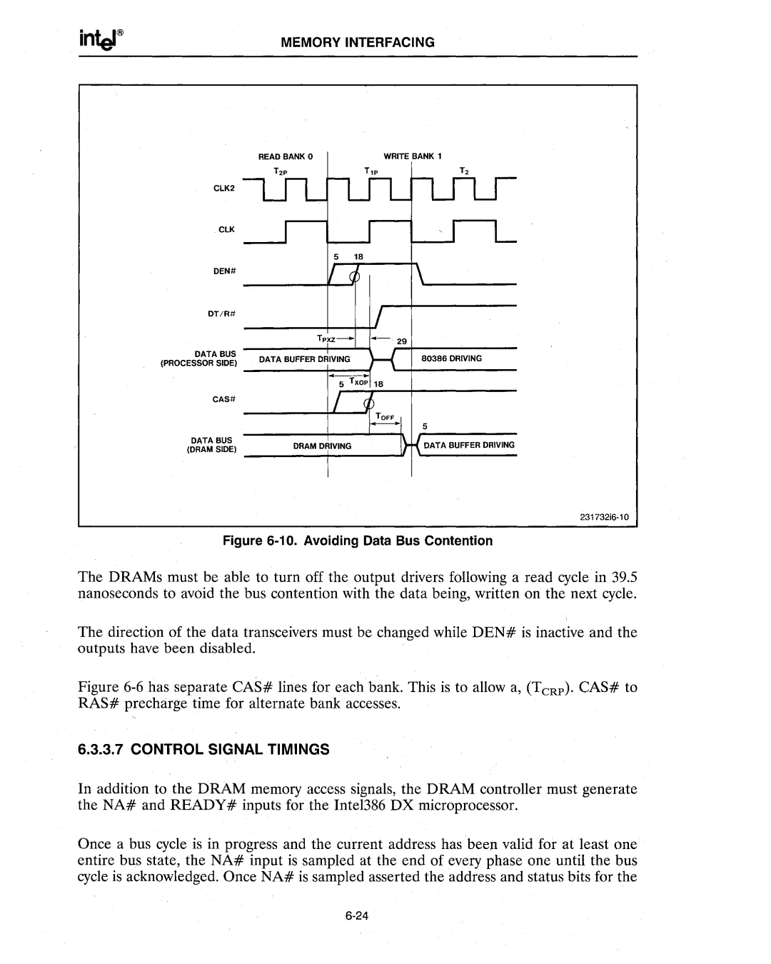
Figure 6-10. Avoiding Data Bus Contention
The DRAMs must be able to turn off the output drivers following a read cycle in 39.5 nanoseconds to avoid the bus contention with the data being, written on the next cycle.
The direction of the data transceivers must be changed while DEN# is inactive and the outputs have been disabled.
Figure 6-6 has separate CAS# lines for each bank. This is to allow a, (TCRP)' CAS# to RAS# precharge time for alternate bank accesses.
6.3.3.7 CONTROL SIGNAL TIMINGS
In addition to the DRAM memory access signals, the DRAM controller must generate the NA# and READY# inputs for the Intel386 DX microprocessor.
Once a bus cycle is in progress and the current address has been valid for at least one entire bus state, the NA# input is sampled at the end of every phase one until the bus cycle is acknowledged. Once NA# is sampled asserted the address and status bits for the