DRAM PLD DESCRIPTIONS
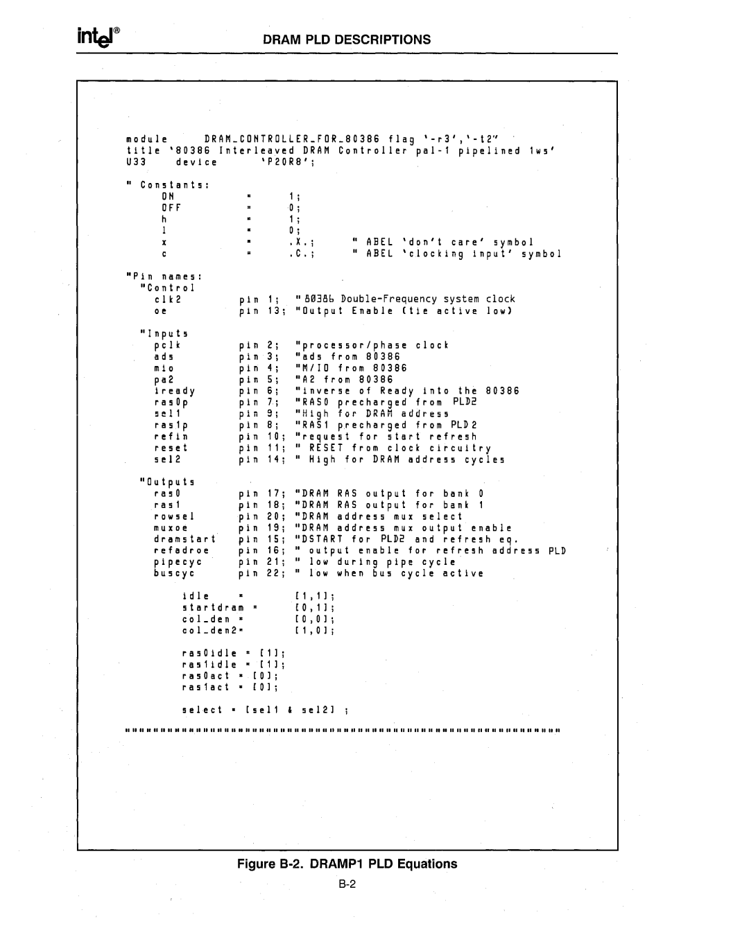
module DRAM_CONTROLLER_FOR_80386 flag ' - r3',' - t2 U
title '80386 Interleaved DRAM Controller
U33 device 'P20R8';
" Constants:
ON1 ;
OFFo;
h1 ;
Io;
•X• ; " ABEL 'don't care' symbol
•C • ; " ABEL 'clacking Input' symbol
"Pin names: "Control
c lk 2 | pin | 1; |
|
oe | pin | 13; | |
"Inputs |
| 2 ; |
|
pc lk | pin |
| |
ads | pin | 3 ; |
|
mlo | pin | 4 ; |
|
pa2 | pin | 5 ; |
|
Iready | pin | 6 ; |
|
r a sOp | pin | 7 ; |
|
5e 11 | pin | S; |
|
raslp | pin | 8 ; |
|
ref I n | pin | 10 ; | |
res e t | pin | 11 ; | |
s e 12 | pin | 14; | |
"Outputs |
| 17 ; | |
r a s 0 | pin | ||
r a s 1 | pin | 18 ; | |
rowsel | pin | 20 ; | |
muxoe | pin | 1S; | |
dramstar( | pin | 15 | ; |
refadroe | pin | 16 | ; |
plpecyc | pin | 21 ; | |
buscyc | pin | 22; | |
"81il386
"processor/phase c lack "ads from 80386
"M/IO from 80386 "A2 from 80386
lIinver5e of Ready In t a the 80386 "RASO precharged from PLD2 "High for DRAM address
"RASI precharged fro m PLD 2 "request for s tar t refresh
"RESET from c lac k circuitry
"High for DRAM address cycles
"DRAM RAS aut put for bank 0 "DRAM RAS output for bank 1 "DRAM address mux s e I e c t
"DRAM address mux output enable "DSTART for PLD2 and refresh e q •
"output enable for refresh address PLD
"law during pipe cycle
"law when bus cycle active
I die |
| [1,1) ; |
startdram | • | [ 0 , 1 ) ; |
cal_den' |
| [ 0 , 0 I ; |
coLden2- |
| [ 1 , 0 I ; |
rasOldle' | [II; |
|
raslldle' | [II; |
|
rasOact • | [01; |
|
ras1act· | [01; |
|
select· [5ell & sel21 ;
