PHYSICAL DESIGN AND DEBUGGING
A
B VIB.I)
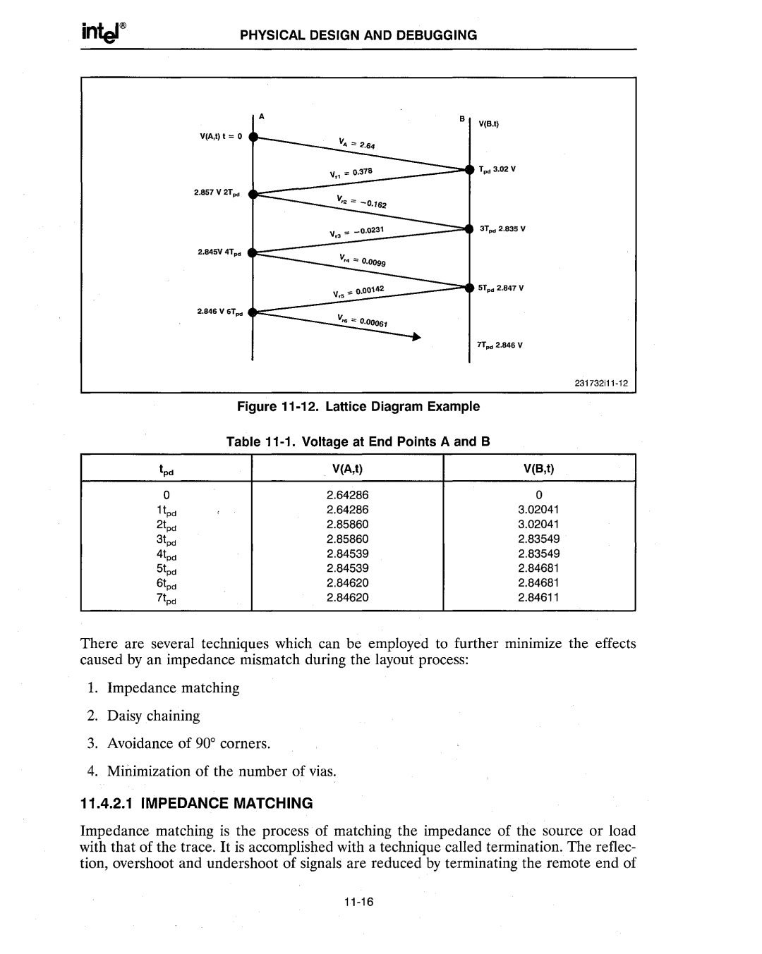
VIA,I) 1=
| 2.857 V 2T... |
|
|
| 2.845V 4Tpo | ||
|
|
| |
| 2.846 V 6Tpd |
| |
| .... |
| |
|
| 7T... 2.846 V | |
|
|
| |
| Figure |
| |
| Table |
| |
tpd |
| V(A,t) | V(8,t) |
0 | . | 2.64286 | 0 |
1tPd | 2.64286 | 3.02041 | |
2tpd |
| 2.85860 | 3.02041 |
3tpd |
| 2.85860 | 2.83549 |
4tpd |
| 2.84539 | 2.83549 |
5tpd |
| 2.84539 | 2.84681 |
6tpd |
| 2.84620 | 2.84681 |
7tpd |
| 2.84620 | 2.84611 |
There are several techniques which can be employed to further minimize the effects caused by an impedance mismatch during the layout process:
1.Impedance matching
2.Daisy chaining
3.Avoidance of 90° corners.
4.Minimization of the number of vias.
11.4.2.1 IMPEDANCE MATCHING
Impedance matching is the process of matching the impedance of the source or load with that of the trace. It is accomplished with a technique called termination. The reflec- tion, overshoot and undershoot of signals are reduced by terminating the remote end of
