MEMORY INTERFACING
•The choice of
.• It is possible to deassert RAS# before the end of the cycle to improve the RAS# precharge time.
•For a single DRAM bank rather than two, the user should tie the DRAMPI PLD A2 input low, leave RASI # unconnected (only RASO# is used), and feed the Intel386 DX microprocessor address bit A2 into the address multiplexer. The DRAMPI PLD equations can be modified to change the RASI # output to duplicate the RASO# output for more drive capability, and the A2 input can be used as another
6.3.4.2USING TAP DELAY LINES
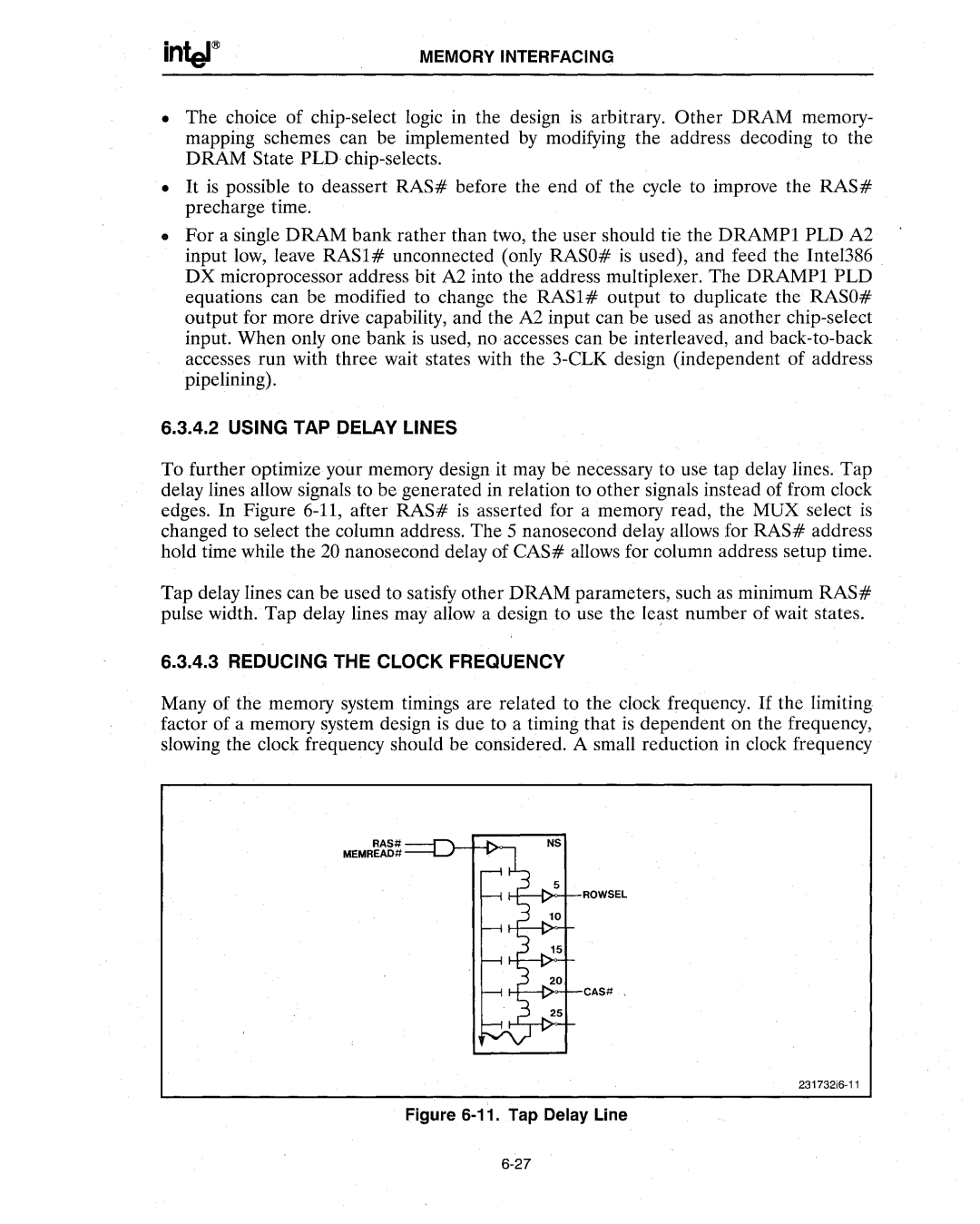
To further optimize your memory design it may be necessary to use tap delay lines. Tap delay lines allow signals to be generated in relation to other signals instead of from olock edges. In Figure
Tap delay lines can be used to satisfy other DRAM parameters, such as minimum RAS# pulse width. Tap delay lines may allow a design to use the
6.3.4.3 REDUCING THE CLOCK FREQUENCY
Many of the memory system timings are related to the clock frequency. If the limiting factor of a memory system design is due to a timing that is dependent on the frequency, slowing the clock frequency should be considered. A small reduction in clock frequency
RAS#NS
MEMREAD#
5
ROWSEL
10
15
20
CAS#
25
