MEMORY INTERFACING
Even if random accesses are made, two DRAM banks allow 50 percent of
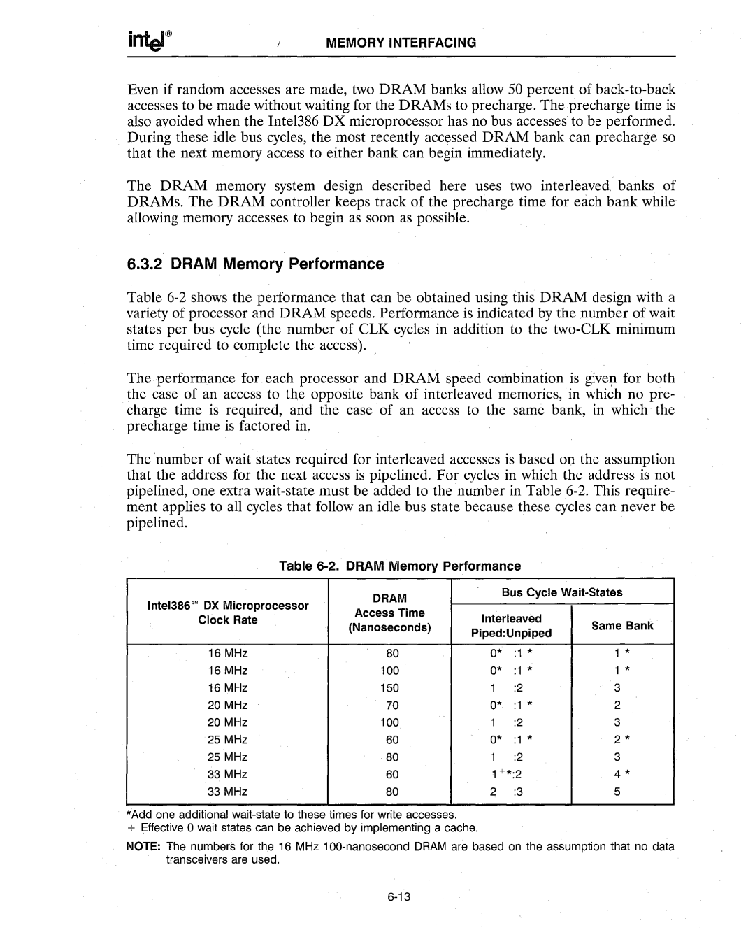
The DRAM memory system design described here uses two interleaved banks of DRAMs. The DRAM controller keeps track of the precharge time for each bank while allowing memory accesses to begin as soon as possible.
6.3.2 DRAM Memory Performance
Table
The performance for each processor and DRAM speed combination is given for both the case of an access to the opposite bank of interleaved memories, in which no pre- charge time is required, and the case of an access to the same bank, in which the precharge time is factored in.
The number of wait states required for interleaved accesses is based on the assumption that the address for the next access is pipelined. For cycles in which the address is not pipelined, one extra
| Table |
| |||
Inte1386'MOX Microprocessor | DRAM |
| Bus Cycle | ||
|
|
| |||
Access Time | Interleaved |
| |||
Clock Rate |
| Same Bank | |||
| (Nanoseconds) | ||||
|
| Piped:Unpiped | |||
|
|
|
| ||
16 MHz |
| 80 | 0* | :1 * | 1 * |
16 MHz |
| 100 | 0* | :1 * | 1 * |
16 MHz |
| 150 | 1 | :2 | 3 |
20 MHz |
| 70 | 0* | :1 * | 2 |
20 MHz |
| 100 | 1 | :2 | 3 |
25 MHz |
| 60 | 0* | :1 * | 2 * |
25 MHz |
| 80 | 1 | :2 | 3 |
33 MHz |
| 60 | 1+*:2 | 4 * | |
33 MHz |
| 80 | 2 | :3 | 5 |
*Add one additional
+Effective 0 wait states can be achieved by implementing a cache.
NOTE: The numbers for the 16 MHz