PHYSICAL DESIGN AND DEBUGGING
AB
T~O
Tpd
2Tpd
3Tpd
4Tpd
5Tpd
rL3rs2V"" ;::. Vr5
6Tpd
...
x
231732i11-11
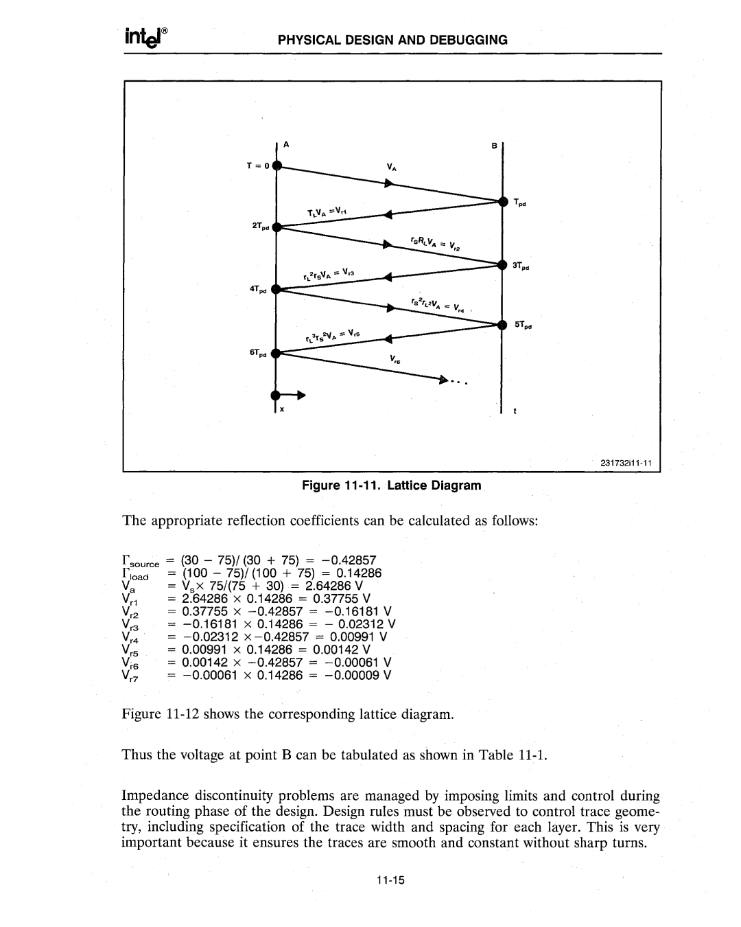
Figure 11-11. Lattice Diagram
The appropriate reflection coefficients can be calculated as follows:
f source = (30 - 75)/ (30 + 75) = -0.42857 f load = (100 - 75)/ (100 + 75) = 0.14286
Va = VsX 75/(75 + 30) = 2.64286 V
Vr1 = 2.64286 X 0.14286 = 0.37755 V
Vr2 = 0.37755 X -0.42857 = -0.16181 V
Vr3 = -0.16181 X 0.14286 = - 0.02312 V
Vr4 = -0.02312 X -0.42857 = 0.00991 V
Vr5 = 0.00991 X 0.14286 = 0.00142 V
V'6 = 0.00142 X -0.42857 = -0.00061 V
Vr7 = -0.00061 X 0.14286 = -0.00009 V
Figure 11-12 shows the corresponding lattice diagram.
Thus the voltage at point B can be tabulated as shown in Table 11-1.
Impedance discontinuity problems are managed by imposing limits and control during the routing phase of the design. Design rules must be observed to control trace geome- try, including specification of the trace width and spacing for each layer. This is very important because it ensures the traces are smooth and constant without sharp turns.
11-15