PHYSICAL DESIGN AND DEBUGGING
|
| 74AS244 |
|
66.67 MHz | 2 |
| 18 |
or 50 MHz | A1 | Y1 | ACLK2 |
OSC | 4 |
| 16 |
| A2 | Y2 |
|
| 6 | Buffer | 14 |
|
| ||
| A3 | Y3 |
|
| 8 | Y4 | 12 |
| A4 | BCLK2 |
G
231732;11·24
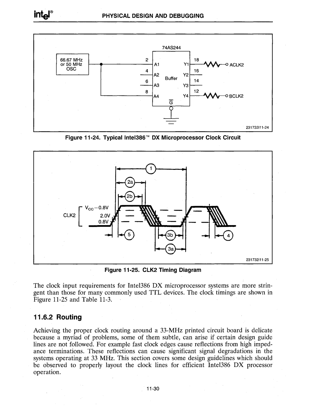
Figure 11·24. Typical Intel386™ DX Microprocessor Clock Circuit
CLK2 [ 2.0V
O.BV
231732;11·25
Figure 11·25. CLK2 Timing Diagram
The clock input requirements for Intel386 DX microprocessor systems are more strin- gent than those for many commonly used TTL devices. The clock timings are shown in Figure
11.6.2 Routing
Achieving the proper clock routing around a