LOCAL BUS CONTROL PLD DESCRIPTIONS
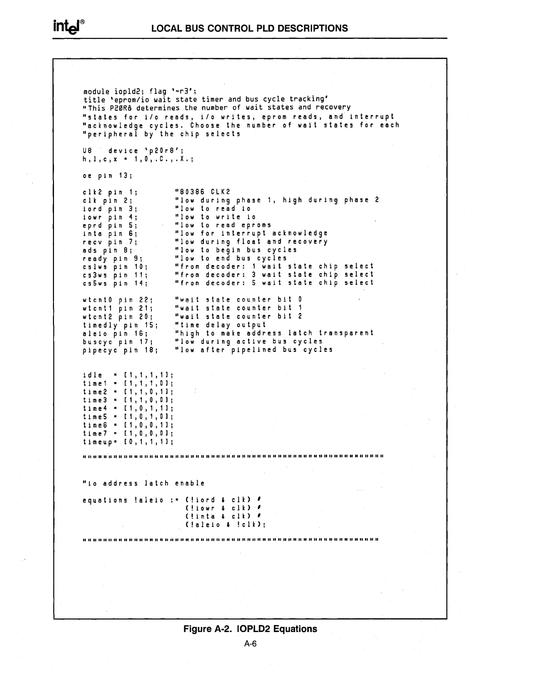
module iopld2; flag
timer and bus cycle tracking' number of wait states and recovery
"states for 1/0 reads, 1/0 writes, eprom reads, and Interrupt "ackn.wledge cycles. Choose the number of wall slales for each "peripheral by Ihe chip selects
U8 device 'p20r8'; h,I,c,x·I,O,.C.,. X.;
oe pin 13;
cI k2 |
| pin |
| 1 ; | "80386 CLK2 | phase | I, | high during | p ha H 2 | ||||
clk | pin | 2 ; | low | during | |||||||||
lor d |
| pin |
| 3 ; | low | to | read | 10 |
|
|
|
| |
lowr |
| pin |
| 4 ; | low | to | wr I t e | 10 |
|
|
|
| |
eprd |
| pin |
| 5 ; | low | 10 | read | eproms |
|
|
| ||
In t a |
| pin |
| 6 ; | low | for | Interrupt acknowledge |
| |||||
recv |
| pin |
| 7 ; | low | during | flo at | and | recovery |
| |||
ads | pin | 8 ; | low to begin bus cycles |
|
| ||||||||
ready | pin | 9 ; | low to end bus cycles |
|
| ||||||||
cslws | pin | 1°; | from | decoder: | 1 | wa It | s I ate | chi p | select | ||||
cs3ws | pin | 11 ; | fro m decoder: | 3 | wa It | 5 ta t e | chi p | Hlecl | |||||
csSws | pin | 14; | from | decoder: | 5 | wall | 5 ta I e | chi p | selecl | ||||
IIlIcnlO pin 22; "wall stat e counter b I I
wlcntl pin 21 ; "walt state counter b I I
wtcnt2 pin 20 ; "wall stale counter b I I
tlmedly pin 15 ; "time delay output
alelo pin 16 ; "high to make address latch transparent
buscyc pin 17 ; II 1ow during active b u 5 cycles
plpecyc pin 18 ; "low a fie r pipellned bU5 cycles
I die • [1, 1 , 1 , 1 ] I 1m e 1 • [1, 1 , 1 , 0 ] Ilme2' [1,1,0,1] Ilme3' [1,1,0,0] tlme4' [1,0,1,1] limeS' [1,0,1,0] tlme6' [1,0,0,1] Ilme7' [1,0,0,0] tlmeup' [0,1,1,1]
"""""""""11""1111""" ""IIIIII"""IIII""""nllll""""IIIIII""""""IIIIII"""""II""
"10 address lalch enable
equations !alelo :. (!Iord clk)
(!Iowr clk) (!Inta' clk) , (!alelo . !clk);
II""""IIUIIIIIIIIII""""IIIIII""""""""""IIIIIIIIII""IIIIII"II""""""'I""""""lllllIn
