PHYSICAL DESIGN AND DEBUGGING
The design of effective decoupling and bypass schemes centers on maximizing the charge stored in the circuit bypass loops while minimizing the inductances in these loops. Some other precautions that can minimize the EMI are as follows:
•Running a ground line in between two adjacent signal lines. The extra line should be grounded at both ends.
•The address and data buses can also be separated by ground lines. This technique may be expensive due to large number of address and data lines.
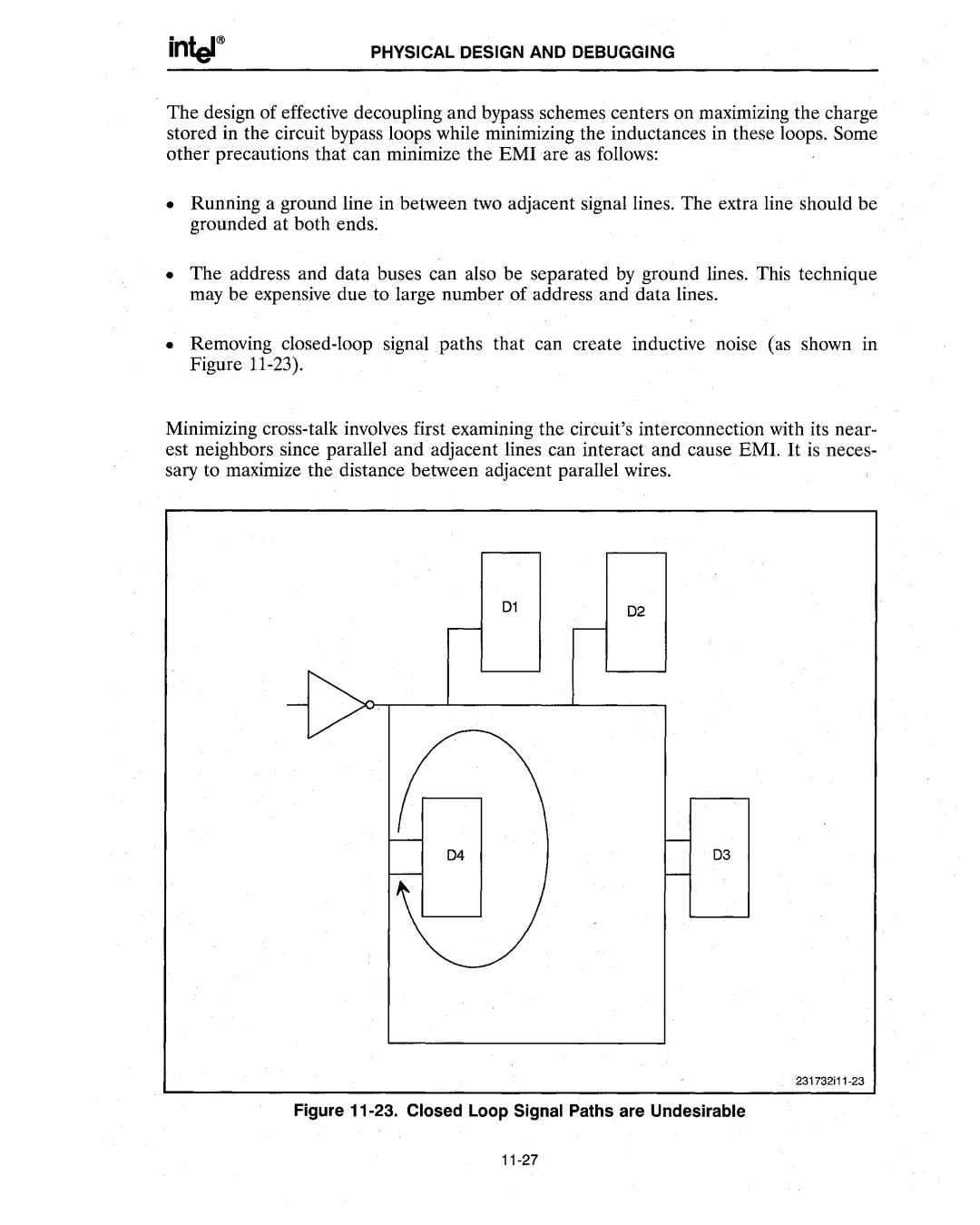
•Removing
Minimizing
0102
03
