MEMORY INTERFACING
WRITE CYCLE
RAS V,H -
V,L -
tWCR
DATA
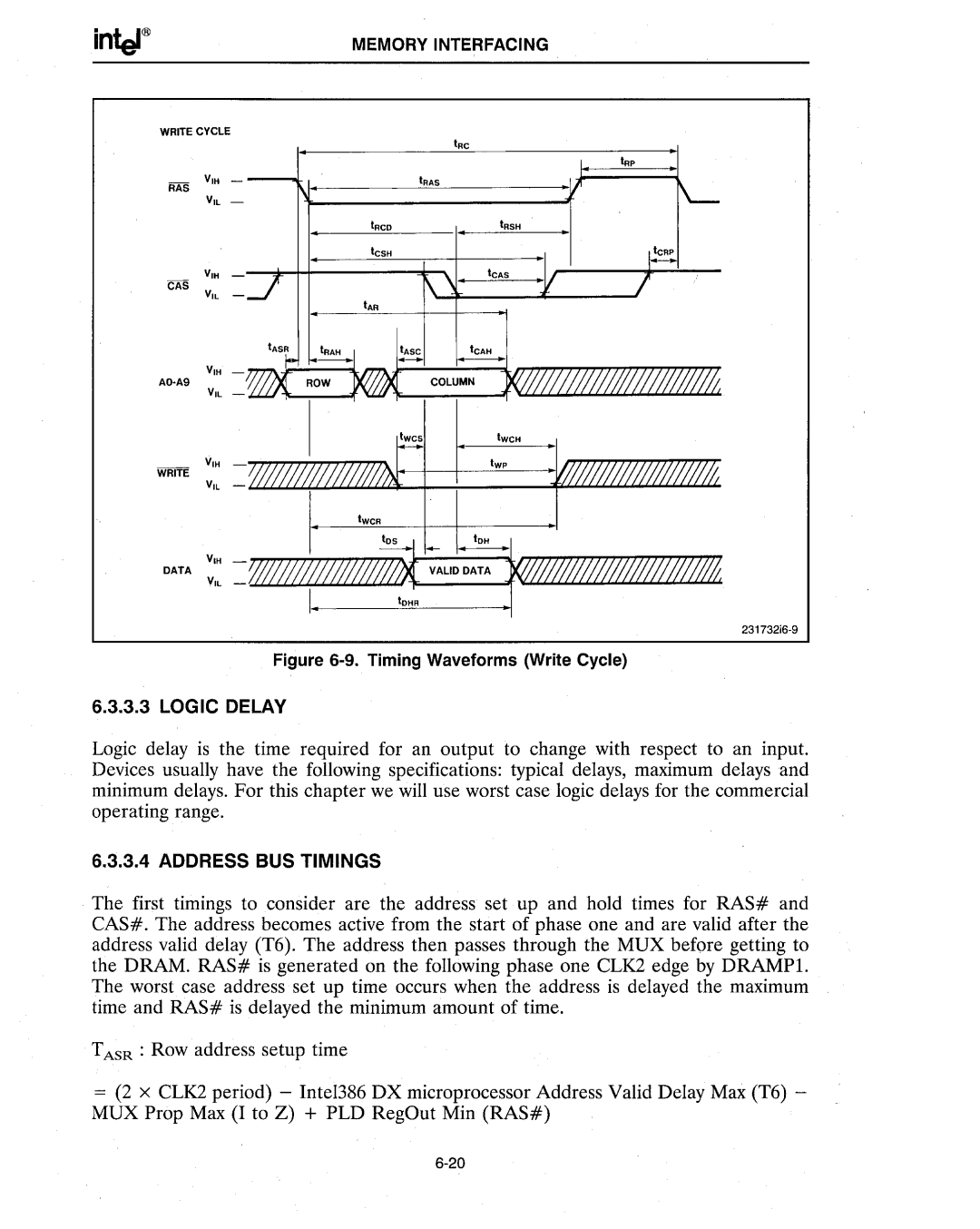
Figure 6-9. Timing Waveforms (Write Cycle)
6.3.3.3 LOGIC DELAY
Logic delay is the time required for an output to change with respect to an input. Devices usually have the following specifications: typical delays, maximum delays and minimum delays. For this chapter we will use worst case logic delays for the commercial operating range.
6.3.3.4 ADDRESS BUS TIMINGS
The first timings to consider are the address set up and hold times for RAS# and CAS# . The address becomes active from the start of phase one and are valid after the address valid delay (T6). The address then passes through the MUX before getting to the DRAM. RAS# is generated on the following phase one CLK2 edge by DRAMPI. The worst case address set up time occurs when the address is delayed the maximum time and RAS# is delayed the minimum amount of time.
TASR : Row address setup time
=(2 x CLK2 period) - MUX Prop Max (I to Z)
Intel386 DX microprocessor Address Valid Delay Max (T6) -
+PLD RegOut Min (RAS#)