MULTIBUS I AND Intel386 DX MICROPROCESSOR
The iLBX bus interface requires the generation of AI, AO, and BHE# from the Inte1386 DX microprocessor BE3#-BEO# outputs.. The iLBX connector contains 24 address bits (AB23-ABO) and 16 data bits (DBlS-DBO), which are taken from the buffered address lines (A23-AO), and data lines (DIS-DO) of the Inte1386 DX micro- processor local bus. BHE# is inverted and buffered to provide the Byte High Enable (BHEN) signal.
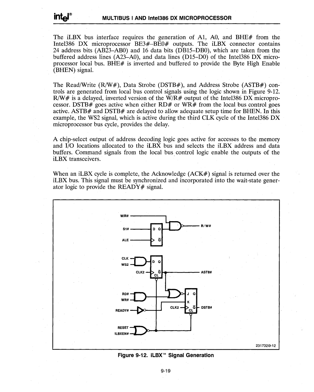
The ReadlWrite (RIW#), Data Strobe (DSTB#), and Address Strobe (ASTB#) con- trols are generated from local bus control signals using the logic shown in Figure 9-12. R1W# is a delayed, inverted version of the W/R# output of the Inte1386 DX micropro- cessor. DSTB# goes active when either RD# or WR# from the local bus control goes active. ASTB# and DSTB# are delayed to allow adequate setup time for BHEN. In this example, the WS2 signal, which is active during the third CLK cycle of the Inte1386 DX microprocessor bus cycle, provides the delay.
Achip-select output of address decoding logic goes active for accesses to the memory and I/O locations allocated to the iLBX bus and selects the iLBX address and data buffers. Command signals from the local bus. control logic enable the outputs of the iLBX transceivers.
When an iLBX cycle is complete, the Acknowledge (ACK#) signal is returned over the iLBX bus. This signal must be synchronized and incorporated into the wait-state gener- ator logic to provide the READY# signal.
W/RII ------- ,
:~:----I~.'..
eLK WS2
....----- ASTBII
RDII | |
WRII | |
READYII -1.>0--+.... | DSTBII |
|
RESET | |
ILBXENII | |
231732i9-12
Figure 9-12. iLBX™ Signal Generation
9-19